
 日本語
日本語

You have a design with more than two layers, and you need a partner who can actually build it, not just quote it. That means real questions: how many layers can they run, what laminate do they stack, what is their true turnaround on a 40-layer board, and how do you tell a capable shop from one that will hand your Gantt chart back to you in shambles?
This guide covers what actually matters when you are sourcing multilayer PCB assembly, including the process, the technical specs worth checking, the real cost drivers, the failure modes nobody warns you about, and a practical checklist for evaluating a multilayer PCB assembly supplier.
What Multilayer PCB Assembly Actually Means
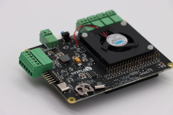
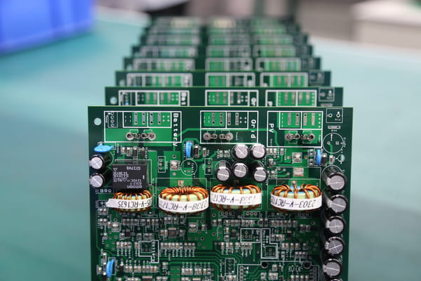
Multilayer PCB assembly is the process of populating and soldering electronic components onto a bare printed circuit board that contains three or more conductive copper layers separated by insulating dielectric material. The layers are interconnected through plated through holes, blind vias, or buried vias, which is what allows a compact board to route far more signal and power paths than a single-sided or double-sided board ever could.
It is worth separating two terms that competitor sites frequently blur together: multilayer PCB fabrication and multilayer PCB assembly.
Fabrication is building the bare, unpopulated board: etching copper, laminating layers, drilling and plating vias, applying solder mask and silkscreen.
Assembly is everything that happens after the bare board exists: solder paste printing, component placement, reflow soldering, through-hole soldering, and inspection.
Many multilayer boards fail not because of a fabrication defect but because of an assembly decision, such as a reflow profile that was never adjusted for the board's thermal mass.
When You Actually Need a Multilayer Design
Not every board needs to go multilayer, and over-speccing adds cost without benefit. Multilayer PCB assembly makes sense when your design hits one or more of these constraints:
Signal density exceeds what 2 layers can route. Once your component count and pin density push routing congestion past a certain point, you either go multilayer or the board grows physically larger, which often is not an option.
You need dedicated ground and power planes. Two-layer boards force ground and signal traces to share space, which increases electromagnetic interference (EMI) and degrades signal integrity. A multilayer stack lets you sandwich signal layers between solid reference planes.
You are running high-speed digital or RF signals. Controlled impedance routing, which is essential above roughly 50 MHz or for any high-speed serial interface (USB3, PCIe, DDR memory buses), requires a defined layer stack-up with known dielectric thickness and reference planes.
Form factor is constrained. Wearables, implantable medical devices, and compact IoT modules often have no room to spread components across a larger single-layer board.
For a simple sensor node with fewer than 100 components and no high-speed interfaces, a 2-layer or 4-layer PCB is often the more practical choice in terms of cost and lead time. Higher layer counts should be selected based on actual requirements, such as routing density, signal integrity, power distribution, and reliability needs
The Multilayer PCB Assembly Process, Step by Step
A competent multilayer PCB assembly workflow follows a sequence that protects signal integrity and mechanical reliability at every stage. Here is the process as it should run on a production floor.
1. Design for Manufacturability (DFM) Review
Before any material is cut, the fabrication and assembly teams should jointly review the Gerber files, stack-up, and BOM. This step catches the majority of downstream defects. A supplier that skips DFM review and jumps straight to production is a red flag, not a sign of speed.
Key DFM checks for multilayer boards include annular ring size on vias, minimum trace and space against the fab's actual capability (not their marketing capability), thermal relief on ground plane connections, and copper balance across layers to prevent warpage during lamination.
2. Stack-Up Design and Material Selection
The layer stack-up defines how signal, ground, and power layers are arranged, and what dielectric material and thickness separate them. This decision drives impedance control, thermal performance, and mechanical rigidity.
Laminate choice matters more than most buyers realize. Mainstream FR-4 works for the majority of designs, but the specific laminate brand and resin system affect glass transition temperature (Tg), dielectric constant consistency, and how well the material survives multiple lamination cycles on high layer count boards. Tier-one Chinese laminate suppliers such as Shengyi and Kingboard are widely used across the industry precisely because their material specs are consistent lot to lot, which matters enormously when you are laminating 20, 30, or 40 layers and cannot afford a delamination failure discovered after assembly.
3. Inner Layer Imaging and Etching
Each inner layer's circuit pattern is transferred via photoresist, exposed, developed, and etched. On high layer count boards, this step is repeated for every internal layer before lamination begins, which is why layer count has such a direct relationship with both cost and lead time.
4. Lamination and Drilling
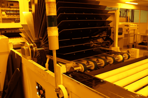
Layers are pressed together under controlled heat and pressure (typically 275 to 400 psi) with prepreg bonding them into a single rigid structure. After lamination, mechanical or laser drilling creates through holes, blind vias, and buried vias, which are then plated to establish electrical connection between layers.
5. Outer Layer Processing, Solder Mask, and Surface Finish
Outer copper layers are imaged and etched, solder mask is applied to protect copper from oxidation and prevent solder bridging, and a surface finish (ENIG, immersion silver, OSP, or lead-free HASL) is applied to the exposed pads.
6. Electrical Testing of the Bare Board
Before assembly starts, the bare multilayer board should undergo flying probe or bed-of-nails testing to verify continuity and detect shorts or opens introduced during fabrication. Skipping this step means you find fabrication defects during assembly, which is far more expensive to diagnose and rework.
7. Solder Paste Printing and SPI
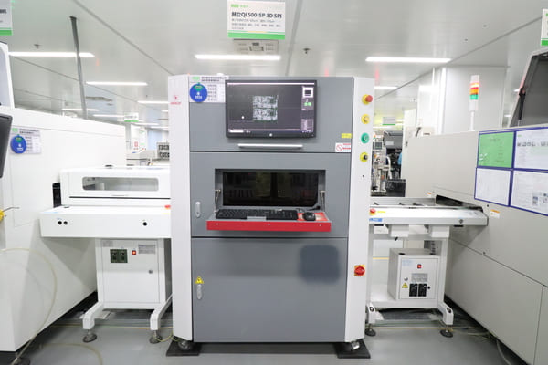
For the assembly phase, solder paste is applied through a laser-cut stencil, and automated solder paste inspection (SPI) verifies paste volume and alignment before any component touches the board.
8. Component Placement
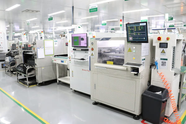
Pick-and-place machines position surface-mount components with micron-level accuracy. On multilayer boards carrying BGAs, micro-BGAs, and fine-pitch components, placement accuracy and machine vision calibration matter more than raw placement speed.
9. Reflow Soldering
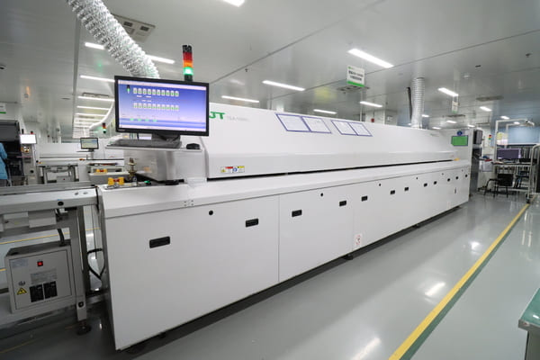
Multilayer boards have significantly higher thermal mass than 2-layer boards because of the additional copper and dielectric layers. This means the reflow thermal profile, the preheat, soak, and reflow zones, must be specifically tuned for the board's layer count and copper weight. Using a generic reflow profile on a high layer count board is one of the most common causes of cold solder joints and incomplete reflow on inner rows of BGA balls.
10. Through-Hole and Selective Soldering
Connectors and mechanically stressed components are typically through-hole mounted and soldered via wave or selective soldering after the SMT stage, adding mechanical strength that pure surface mount cannot provide.
11. Inspection and Testing
A rigorous multilayer PCB assembly process includes automated optical inspection (AOI) for placement defects, X-ray inspection for hidden joints under BGAs and for verifying buried via integrity, in-circuit testing (ICT) for electrical verification, and functional testing that simulates real operating conditions.
12. Final QA and Packaging
Visual and dimensional checks, cleaning to remove flux residue, and moisture-barrier or anti-static packaging close out the process before the boards ship.
Technical Capabilities to Verify Before You Quote
| Parameter | Typical Industry Range | Why It Matters |
|---|---|---|
| Layer Count | 4 to 40+ layers | Higher layer counts require more lamination cycles and tighter registration control. |
| Laminate Materials | FR-4, high-Tg FR-4, Rogers, polyimide | Determine thermal performance, dielectric consistency, and signal integrity. |
| Copper Weight | 0.5 to 4 oz (inner), 1 to 20 oz (outer) | Heavier copper supports higher current but makes fine-pitch etching more challenging. |
| Minimum Trace/Space | 3 to 8 mil (down to ~2.75 mil for advanced shops) | Determines the routing density achievable within the available layer count. |
| Via Types | Through-hole, blind, buried, microvia (HDI) | Blind and buried vias increase routing density but add fabrication cost and complexity. |
| Board Thickness | 0.4 mm to 6 mm+ | Must match connector specifications and enclosure mechanical requirements. |
| Surface Finish | ENIG, ENEPIG, immersion silver, OSP, lead-free HASL | Affects solderability, shelf life, and compatibility with gold-wire bonding when required. |
| Certifications | ISO 9001, IPC-6012 Class 2/3, AS9100, ITAR (defense) | Verify manufacturing process control, quality management, and traceability. |
What Actually Drives Multilayer PCB Assembly Cost
Buyers are often surprised that two quotes for the "same" board can differ by 30 to 50 percent. Here is what is actually driving that spread.
1. Layer count. Cost scales roughly with the number of lamination and imaging cycles, not linearly with layer count, but each additional pair of layers adds meaningful cost.
2. Laminate material. Standard FR-4 is the cost baseline. High-Tg FR-4, Rogers RF laminates, and polyimide all carry a premium, sometimes substantial.
3. Via complexity. Simple through-hole vias are the cheapest. Blind and buried vias require sequential lamination cycles and add both cost and lead time. Microvias for HDI designs cost more still.
4. Copper weight and trace/space. Heavy copper and fine trace/space push a fab closer to its process limits, which reduces yield and raises cost.
5. Quantity and panel utilization. Prototype quantities (1 to 50 pieces) carry a much higher per-unit cost than production runs because setup and tooling costs are amortized over fewer boards.
6. Turnaround time. Standard lead time versus expedited or same-day service can add 30 to 100 percent to the price, depending on how much the fab has to disrupt its production schedule.
7. Testing and certification requirements. ICT, functional test fixtures, and certifications like ITAR registration or AS9100 for aerospace all add cost, and rightly so given the traceability they provide.
If a quote comes in dramatically below every competitor for the same spec sheet, ask specifically what laminate brand, what via structure, and what testing is included. Under-speccing a quote to win business and then substituting materials is a known industry problem, and it is exactly why verifying laminate brand (for example, confirming a supplier is genuinely using Shengyi or Kingboard material rather than an unnamed generic substitute) is worth doing before you commit a production order.
Lead Time: What Is Realistic and What Is Marketing
Lead time on multilayer PCB assembly depends heavily on layer count and via complexity, not just order volume.
Simple 4 to 8 layer boards, standard vias: typically 5 to 10 business days for fabrication plus 2 to 5 days for assembly under normal scheduling.
12 to 20 layer boards, or boards with blind/buried vias: commonly 10 to 15 business days for fabrication alone, because of sequential lamination.
High layer count boards (24 to 40 layers): can run 3 to 4 weeks or more through fabrication depending on the shop's press capacity and sequential lamination requirements.
However, professional PCB manufacturers like PCBgogo can provide 24-hour fast-turn PCB assembly services for eligible prototypes and small-batch projects, helping engineers speed up the process from design to finished boards and meet demanding project timelines.
Common Multilayer PCB Assembly Defects and How to Prevent Them
This is the section most competitor pages skip entirely, and it is usually the difference between a smooth production run and a costly field failure.
1. Delamination
What it is: Separation between layers, often appearing as blistering or a measles pattern under thermal stress.
Root cause: Usually moisture absorption in the laminate before reflow, insufficient lamination pressure or temperature, or a Tg rating too low for the reflow profile the board will see.
Prevention: Bake boards before assembly if they have been stored in humid conditions, verify laminate Tg against your actual reflow peak temperature (lead-free reflow commonly peaks around 245 to 260°C), and confirm the fab's lamination press parameters are logged and consistent per panel, not eyeballed.
2. Warpage and Bow/Twist
What it is: The board deviates from flat, which causes uneven stencil contact during paste printing and coplanarity issues during component placement, especially for BGAs.
Root cause: Uneven copper distribution across layers (copper balance), asymmetric stack-up, or uneven cooling after lamination.
Prevention: A good DFM review checks copper balance layer to layer before fabrication starts. IPC-6012 specifies acceptable bow and twist limits (generally under 0.75% for boards with surface mount components); ask your supplier what they measure to and how.
3. Interlayer Misregistration
What it is: Inner layers shift slightly relative to each other during lamination, causing vias to miss their intended pad or annular ring on internal layers.
Root cause: Tooling pin wear, material shrinkage inconsistency, or excessive layer count without adequate registration control.
Prevention: X-ray inspection specifically targeting buried via alignment, not just BGA solder joints, is the only reliable way to catch this before the board ships. Ask explicitly whether X-ray inspection scope includes buried via verification.
4. Incomplete Reflow on Inner BGA Rows
What it is: Outer BGA balls reflow properly, but inner rows show cold or incomplete joints, often invisible without X-ray.
Root cause: A reflow thermal profile tuned for a low-mass board applied to a high layer count board with much greater thermal mass, so heat does not penetrate to the board core in time.
Prevention: Thermal profile should be re-validated per stack-up, not reused from a different job. This is a process discipline question worth asking any assembler directly: do they re-profile reflow per board design, or reuse a standard profile across jobs.
5. Via Reliability Failures Under Thermal Cycling
What it is: Plated through-hole or via barrel cracking after repeated thermal cycling in the field, common in automotive and industrial applications.
Root cause: Insufficient copper plating thickness in the via barrel, or aspect ratio (board thickness to via diameter) pushed beyond the fab's reliable process window.
Prevention: For high reliability applications, specify IPC Class 3 and request via barrel plating thickness data, not just a pass/fail statement.
How to Choose a Multilayer PCB Assembly Supplier
Use this checklist when evaluating quotes, rather than defaulting to whoever responds fastest or quotes lowest.
1. Ask for documented layer count and material capability, not a marketing number. A shop that lists up to 40 layers should be able to show you a recent job at that layer count.
2. Confirm laminate brand transparency. Reputable suppliers will name their material source (Shengyi, Kingboard, Isola, Rogers, etc.) rather than saying high-quality FR-4.
3. Ask what DFM review actually includes. A checkbox DFM process and a real engineering review that flags copper balance, thermal relief, and impedance concerns are very different things.
4. Verify testing scope in writing. AOI is standard; ask specifically whether X-ray covers buried vias and BGA joints, and whether ICT or functional test is included or an add-on.
5. Check whether assembly and fabrication happen in-house or are outsourced. A supplier running both under one roof, like PCBgogo's own manufacturing facility, generally gives tighter quality control and fewer handoff errors than a broker coordinating between separate fab and assembly vendors, since there is one team accountable for the whole board rather than finger-pointing between two companies when a defect surfaces.
6. Get a real quote for your actual stack-up, not a generic per-layer estimate. Suppliers with transparent online quoting tools that account for via type, copper weight, and material let you sanity-check pricing before committing a purchase order.
7. Ask about expedite options and what they specifically cover. As noted above, get clarity on which stage a 24 hour or quick-turn claim applies to.
8. Request references or case studies in your actual industry. Aerospace, medical, and industrial multilayer boards have very different reliability bars than consumer electronics, and a supplier's experience should match your application.
Multilayer PCB Assembly vs. Single and Double Layer PCBs
| Feature | Single/Double Layer PCB | Multilayer PCB |
|---|---|---|
| Layer count | 1 to 2 | 3 or more |
| Routing density | Limited | High |
| Signal integrity | Basic | Excellent, with dedicated ground/power planes |
| EMI control | Minimal | Strong, via plane shielding |
| Typical cost | Lowest | Higher, scales with layer count |
| Typical lead time | Fastest | Longer, scales with layer count and via complexity |
| Best for | Simple, low-density circuits | High-speed, high-density, or space-constrained designs |
Frequently Asked Questions
What is multilayer PCB assembly?
Multilayer PCB assembly is the process of mounting and soldering electronic components onto a printed circuit board that has three or more layers of copper conductors separated by insulating material, with layers connected through plated vias.
How many layers can a multilayer PCB have?
Standard multilayer PCBs commonly range from 4 to 20 layers. Advanced fabricators can produce boards up to 40 layers or more, though very high layer counts require sequential lamination and specialized process control, which adds cost and lead time.
How much does multilayer PCB assembly cost?
Cost depends primarily on layer count, laminate material, via complexity (through-hole versus blind/buried), copper weight, and order quantity. A simple 4-layer prototype run costs significantly less per unit than a 20+ layer board with blind vias and heavy copper, and prototype quantities always carry a higher per-unit cost than production volumes.
What is the difference between multilayer PCB fabrication and multilayer PCB assembly?
Fabrication builds the bare, unpopulated board through etching, lamination, and drilling. Assembly is the subsequent process of placing and soldering components onto that finished bare board. Some suppliers only do one or the other; verifying a supplier handles both in-house reduces handoff risk.
What causes delamination in multilayer PCBs?
Delamination is typically caused by moisture absorbed into the laminate before reflow, insufficient lamination pressure or temperature during fabrication, or a laminate Tg rating that is too low for the reflow temperatures the board experiences during assembly.
Is a higher layer count always better?
No. Layer count should match the electrical and mechanical requirements of the design. Over-speccing layer count adds cost and lead time without functional benefit if the routing density and signal integrity requirements do not call for it.
How do I find a reliable multilayer PCB assembly supplier?
Look for documented capability at your required layer count, transparency about laminate material sourcing, a real DFM review process, clear testing scope including X-ray verification of buried vias, and ideally in-house fabrication and assembly under one roof to reduce handoff errors. Suppliers such as PCBgogo, which fabricates up to 40 layers using Shengyi and Kingboard laminates in a self-operated facility, are worth including in your comparison specifically because they publish these specifics rather than making generic capability claims.
What is a typical lead time for multilayer PCB assembly?
Simple 4-layer to 8-layer boards typically run 5 to 10 business days for fabrication plus a few additional days for assembly. High layer count boards with blind or buried vias can take 3 to 4 weeks or longer through fabrication alone due to sequential lamination cycles.
Final Takeaway
High-quality multilayer PCB assembly depends on more than just the number of layers — it requires precise engineering control at every stage, from DFM review and stack-up planning to assembly and inspection. Choosing a supplier with proven manufacturing capabilities, transparent processes, and reliable quality control can make a significant difference in your project success.
Ready to bring your multilayer PCB project to production? Upload your Gerber files now to get a quote. Talk to PCBgogo's engineering team about your stack-up and reflow requirements and get expert support from prototype to volume manufacturing.





