日本語

QUICK ANSWER PCB etching is the process of removing unwanted copper from a laminate to form the circuit pattern defined by the photoresist layer. Most standard PCBs use wet chemical etchants such as ferric chloride, cupric chloride, or alkaline solutions, while dry etching and laser ablation are used for advanced HDI, fine-pitch, and RF designs where tighter side-etch control is required. Maintaining the correct etch factor and trace geometry is essential to keep the finished board within design tolerances.
What is PCB Etching
Etching is the step that turns a copper-clad laminate into an actual circuit. A resist layer — dry film photoresist for most production boards, liquid or screen-printed resist for simpler jobs — protects the copper that will become traces and pads. Everything left exposed gets dissolved or ablated away in the etch stage, and what's left after stripping the resist is the finished conductor pattern.
From an engineering standpoint, etching isn't just a chemical strip step — it's a dimensional control step. Every etch process removes copper both downward (through the intended thickness) and sideways (under the resist edge, called undercut or side etching). The ratio between those two determines whether a 4-mil trace comes out at 4 mils or at 3.6 mils with rounded sidewalls that quietly change impedance.
How Does the PCB Etching Process Work?
PCB etching transforms a copper-clad laminate into a usable circuit pattern. Although production equipment varies, the process follows six basic steps.
Step 1: Prepare and Clean the Copper Surface
The copper surface must be free of oxidation, grease, dust, and fingerprints. Even small contaminants can prevent the resist from bonding properly, creating pinholes, broken traces, or unwanted copper after etching.
The board is normally cleaned, rinsed, and dried immediately before the resist is applied. Once cleaned, the copper surface should not be touched with bare hands.
Step 2: Apply the Circuit Pattern
An etch-resistant pattern protects the copper that must remain as traces, pads, and planes. Common pattern-transfer methods include:
Dry-film photoresist for accurate, repeatable production
Liquid photoimageable resist for coating complex surfaces
Screen-printed resist for suitable production applications
Toner transfer or resist pens for simple prototypes
The method should match the required line width, production volume, and registration accuracy. Toner transfer is convenient for basic prototypes but is generally less consistent than photoimaging.
Step 3: Expose and Develop the Resist
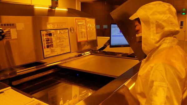
For photoresist processes, the circuit image is transferred by exposing the coated board through a phototool or by direct imaging. The board is then developed to uncover the copper that must be removed.
Exposure and development must be balanced. Underexposure can produce weak or incomplete features, while excessive exposure or development may distort fine traces and spacing. Before etching begins, the operator should inspect the resist for scratches, pinholes, lifting edges, and incomplete development.
Step 4: Etch the Exposed Copper
The board is exposed to an etchant that dissolves unprotected copper while the resist protects the required circuit pattern.
Small-scale operations may use immersion tanks, while industrial manufacturers typically use spray or conveyorized etching equipment. Spray systems continually bring active solution into contact with the copper, improving etch speed and uniformity.
Temperature, chemical condition, copper loading, spray pressure, and exposure time must be controlled together. The process should stop as soon as the unwanted copper has been removed. Leaving the board in the etchant longer than necessary increases undercut and can make finished traces narrower than designed.
Step 5: Rinse and Strip the Resist
The board is rinsed promptly to stop the chemical reaction and prevent etchant from being carried into later processes. The remaining resist is then stripped to reveal the finished copper pattern.
Incomplete rinsing or stripping can leave residues that interfere with inspection, surface finishing, solder mask adhesion, or later plating processes. Rinse water and spent chemicals must be handled according to the applicable waste-management requirements.
Step 6: Inspect the Copper Pattern
Inspection confirms that the etched circuit matches the design. Depending on the board and quality requirements, this may include:
Visual inspection for residual copper, pinholes, and damaged traces
Automated optical inspection to compare the pattern with design data
Trace-width and spacing measurements at critical locations
Continuity and isolation testing for opens and shorts
Microsection analysis when conductor geometry must be verified
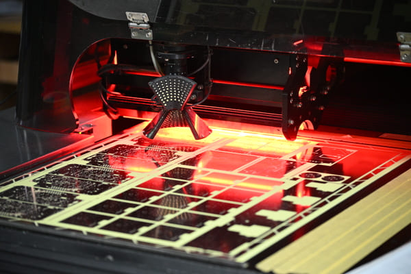
A useful process-control practice is to measure representative traces near the panel edges, center, dense circuitry, and open copper areas. This helps detect local over-etching or uneven etching that a single measurement could miss.
PCB Etching Methods: Applications, Advantages, and Limitations
Before selecting an etching process, it is important to understand how each method differs in precision, production capacity, cost, and process control. The following table provides a practical comparison of the main PCB etching methods.
| Method | How It Works | Typical Use | Strength | Limitation |
|---|---|---|---|---|
| Wet Chemical Etching | Uses a chemical solution to remove exposed copper | Most subtractive PCB manufacturing processes | Mature, efficient, and suitable for volume production | Causes undercut and requires chemical-waste management |
| Spray Etching | Continuously sprays fresh etchant onto the copper surface | Industrial PCB production lines | Provides better etch speed and uniformity | Requires specialized equipment and precise process control |
| Immersion Etching | Submerges the PCB in an etchant solution | DIY projects, laboratories, and low-volume production | Simple equipment and low setup cost | Slower mass transfer and less consistent etching |
| Plasma/Dry Processing | Uses plasma or reactive gases to treat or remove material | Special materials, surface cleaning, and microfabrication | Offers directional processing and precise control | Not a common replacement for conventional etching of thick copper |
| Laser Ablation | Uses a focused laser to remove or modify material directly | Rapid prototyping and specialized fabrication | Digital, flexible, and may not require a conventional mask | Limited throughput, possible heat effects, and high equipment cost |
In practice, wet chemical etching remains the primary choice for conventional PCB production, while plasma and laser processes are generally reserved for specialized applications.
Common PCB Etching Defects and How to Fix Them
Even when the correct etching method and chemical are selected, unstable process conditions can still cause defective copper patterns. The following table helps identify common PCB etching defects and their most likely solutions:
| Defect | What It Looks Like | Likely Causes | Corrective Actions |
|---|---|---|---|
| Over-Etching | Narrow traces, reduced pads, or open circuits | Excessive etching time, high temperature, or insufficient artwork compensation | Reduce etching time, stabilize the solution, and adjust trace compensation |
| Under-Etching | Residual copper or shorts between adjacent traces | Exhausted etchant, low temperature, insufficient spray pressure, or excessive conveyor speed | Check the etchant condition, clean the nozzles, and adjust the conveyor speed |
| Excessive Undercut | Copper is removed laterally beneath the resist | Thick copper, prolonged etching, or poor resist performance | Optimize copper thickness, spray conditions, etching time, and resist quality |
| Pinholes | Small holes, weak spots, or breaks in copper features | Contaminated copper or defects in the resist | Improve surface cleaning and inspect the resist before etching |
| Uneven Etching | Different areas of the panel etch at different rates | Blocked nozzles, trapped air, or uneven pattern density | Maintain the equipment and optimize panel orientation and spray distribution |
| Resist Lifting | Pattern edges peel away during etching | Poor surface preparation, weak adhesion, or chemical incompatibility | Improve pre-cleaning and confirm resist compatibility |
| Ragged Edges | Rough or irregular trace boundaries | Imaging errors, damaged resist, or unstable etchant conditions | Check the artwork, exposure, development, and chemical controls |
But most etching defects are easier to prevent than to repair. Monitoring trace dimensions, etchant condition, temperature, and equipment performance can reveal process drift before it affects an entire production batch.
Side Etching on an HDI PCB: A Practical Example
A recurring scenario in HDI fabrication illustrates why etch factor control matters more than etchant selection alone. Consider a typical 8-layer HDI design with 3.5-mil traces and 4-mil spacing for a 5G RF front-end module. Designed for 50-ohm single-ended impedance, the board is highly sensitive to any undercut: even 0.3–0.4 mils of extra side etching per edge is enough to widen the gap between adjacent traces and pull impedance outside a ±10% window, which shows up downstream as return-loss and insertion-loss deviations during RF testing rather than as a visible defect.
The practical fix isn't a different etchant — it's catching the risk before etching starts. A DFM review flags trace-to-copper-thickness ratios that are tight for the intended etch process, spray-etch parameters get adjusted to raise the etch factor for that specific layer, and AOI inspection after etch — checking line width and spacing against the original artwork — confirms the correction held before the board moves to lamination. That sequence, not the choice of chemical, is what keeps fine-pitch RF boards in spec.
PCBgogo - Reliable, High-Quality PCB Manufacturing
PCBgogo combines advanced etching technology with precise process control to create clean, well-defined traces with minimal undercut and fewer defects. Careful post-etch inspection ensures the consistent, high-quality results required for demanding PCB designs.
Get a Free Quote >
FAQ
1. What's the most common cause of etching defects on production boards?
Inconsistent resist adhesion is the most frequent root cause — even minor lifting at the resist edge lets the etchant undercut copper that was supposed to be protected, producing thin or broken traces.
2. Does etching affect impedance control?
Yes. Side etching narrows trace width and rounds the cross-section, both of which shift characteristic impedance — this matters most on RF and high-speed differential-pair layers with tight tolerance budgets.
3. Is dry etching always better than wet etching?
No — dry etching gives tighter tolerances but costs more and runs slower for bulk copper removal. Wet etching remains the right choice for standard trace widths above roughly 6 mils.
4. How do manufacturers verify etching quality before a board ships?
Post-etch AOI checks line width and spacing against the original artwork, and cross-section or micro-section testing confirms copper thickness and sidewall profile fall within the specified tolerance class.
5. Can I compensate my design for expected etch undercut?
Yes — designers commonly widen trace artwork slightly (etch compensation) based on the fabricator's known etch factor for a given copper weight, so the finished trace lands at the intended width.
6. Does copper thickness change how long etching takes?
Yes — heavier copper (2 oz/70 microns) requires longer etch dwell time or a more aggressive process than standard 1 oz copper, and that extra dwell time increases the risk of side etching if not compensated for.