
 日本語
日本語

If you are sourcing a multilayer PCB manufacturer for the first time, the question is rarely "what is a multilayer PCB." It is closer to this: can this factory actually build my stack-up, hit my tolerance, and ship on the date I need, without a surprise change order three weeks in. This guide answers that question directly. It walks through the full multilayer PCB manufacturing process the way a fabrication engineer actually runs it on the shop floor, then adds what most articles on this topic leave out: real cost drivers, realistic lead times by layer count, a DFM checklist you can hand to your layout team, and a framework for evaluating any multilayer PCB manufacturer before you commit a purchase order.
I have spent years reviewing stack-ups, chasing lamination voids, and explaining to customers why their 20-layer board costs four times more than their 4-layer board. Everything below reflects that hands-on experience, not a rewritten datasheet.
What a Multilayer PCB Is and Why Layer Count Matters?
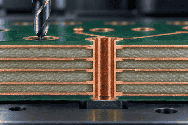
A multilayer PCB is any circuit board built from three or more conductive copper layers, separated by insulating dielectric material and bonded into a single rigid structure under heat and pressure. The moment you go beyond two layers, you are no longer just etching copper on a laminate. You are building a laminated composite, and every layer you add changes the thermal behavior, the drilling difficulty, and the electrical performance of the whole board.
Consumer electronics like smartphones typically run 8 to 12 layers. Industrial control boards commonly sit at 6 to 10 layers. High-end networking, aerospace, and server backplane designs can run 20, 30, or even 40+ layers. The manufacturing process described below scales across that entire range, but the difficulty, cost, and defect risk do not scale linearly. A 12-layer board is not "three times harder" than a 4-layer board. It is closer to ten times harder, because tolerance stack-up, drill aspect ratio, and lamination symmetry all compound.
The Multilayer PCB Manufacturing Process, Step by Step
This is the actual production sequence used on a rigid FR-4 multilayer board with plated through-holes. Blind vias, buried vias, and HDI microvias add extra cycles, which I cover separately below.
1. Engineering Data Review and DFM
Fabrication starts when the factory receives Gerber, ODB++, or IPC-2581 files along with the drill file and stack-up request. A competent CAM engineer runs a Design for Manufacturability check before anything touches a panel. This step catches the errors that would otherwise ruin an entire panel: trace widths below the process floor, annular rings too small for the drill tolerance, acid traps, and impedance targets that do not match any realistic dielectric combination.
A manufacturing traveler is generated at this stage. It follows the physical panel through every process step, recording raw material lot numbers, press cycle parameters, and inspection checkpoints. This traceability record is what lets a factory answer the question "which panel and which press cycle produced this board" months later if a field failure comes back.
2. Material Selection and Stack-Up Design
The engineer selects core and prepreg thickness to hit your target finished thickness, typically 1.6 mm, while balancing copper distribution across the stack. Standard multilayer boards use FR-4 epoxy glass laminate. High-speed or RF designs move to lower-loss materials such as Rogers RO4000 series or PTFE-based laminates, which carry dielectric constants around 2.2 to 3.5 versus FR-4's 4.2 to 4.6.
Material sourcing quality matters more here than most buyers realize. Two boards can use "FR-4" on paper and behave completely differently under thermal cycling if the resin system, glass weave, and copper foil come from different tiers of supplier. This is one area where I tell customers to ask directly which laminate brand their fabricator uses. Reputable Chinese and Taiwanese factories typically source from established laminate makers such as Shengyi Technology or Kingboard, both of which publish full material data sheets for Tg, CTE, and dielectric constant. A manufacturer that cannot name its laminate supplier, or that swaps suppliers between orders without telling you, is a genuine risk to long-term reliability, especially for boards that will see thermal cycling in the field.
A balanced stack-up, where copper distribution and dielectric thickness are close to symmetric top to bottom, resists warping during lamination and costs less to produce than an unbalanced one. If your design allows any flexibility in layer arrangement, ask your fabricator to review the stack-up for balance before you release it.
3. Inner Layer Imaging and Etching
Each inner layer starts as a copper-clad core. The core is cleaned, then coated with a photoresist film. A phototool or laser direct imaging (LDI) system exposes the circuit pattern onto the resist. LDI has become the standard for anything below 4 mil (0.1 mm) trace and space, because it eliminates the registration error inherent in physical phototools.
After exposure and development, the panel goes through an etch bath, typically ferric chloride or cupric chloride, which removes all copper not protected by hardened resist. The remaining resist is stripped, leaving the finished circuit pattern in copper. Every inner layer then passes through Automated Optical Inspection (AOI) before it is allowed anywhere near a lamination press. Catching an open or a short at this stage costs pennies. Catching the same defect after lamination means scrapping an entire multilayer panel, which is why AOI at the inner-layer stage is non-negotiable at any factory worth using.
4. Lamination
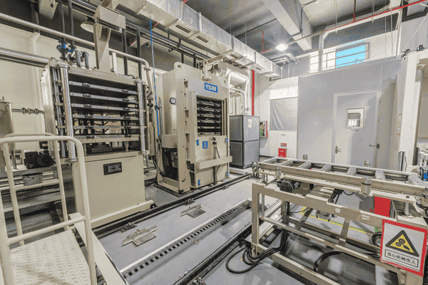
This is the step that actually makes a multilayer board "multilayer." Inner layer cores and sheets of prepreg (uncured, resin-impregnated fiberglass) are stacked in the exact sequence defined by the stack-up, oxide-treated on the copper surface first to improve adhesion, then loaded into a hydraulic press.
Heat, typically around 175 to 185°C, and pressure, typically 350 to 500 psi, are applied for a full press cycle. The prepreg resin melts, flows to fill the gaps between layers, and cures into a solid bond. A standard lamination cycle runs 4 to 6 hours. Boards with blind or buried vias require additional lamination cycles, one per set of buried layers, because those layers must be drilled, plated, and bonded before the next set of layers is added on top. This is the single biggest reason a 12-layer board with buried vias can take longer to fabricate than a 20-layer board without them.
Registration accuracy during lamination directly determines whether your vias land where they should on every layer. A misalignment of even a few thousandths of an inch across a 20-layer stack can break the connection between a via and an inner-layer pad, and that failure mode is invisible until electrical test.
5. X-Ray Registration Check and Drilling
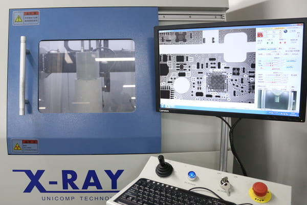
Before drilling, the laminated panel is X-rayed to confirm the internal layers are properly registered to the drill program. Skipping this step on a high-layer-count board is how you get a batch of boards with broken via connections that nobody catches until final test.
Drilling uses mechanical carbide drills for standard through-holes, typically 0.2 to 0.5 mm in diameter, and laser drilling for microvias below 0.15 mm, which is standard on HDI boards. Drilling generates heat that can smear melted resin across the exposed copper inside the hole. This smear has to be removed with a desmear or etchback process before plating, or the copper plating in the next step will not bond properly and you get an intermittent, temperature-sensitive open circuit that is one of the hardest field failures to diagnose.
6. Copper Plating
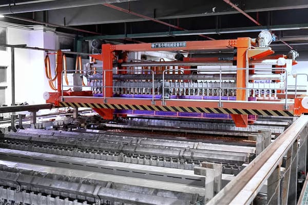
Electroless copper deposits a thin seed layer of conductive copper across the entire hole wall, since the drilled hole starts as bare fiberglass and resin with no conductivity. Electrolytic copper plating then builds this up to the target thickness, typically 20 to 35 microns in the barrel of the via, to create a reliable electrical connection between layers.
Plating thickness distribution across a panel is a real quality differentiator between factories. Uneven plating, thicker at the panel edges and thinner in the center, is a common defect on poorly controlled lines and shows up later as vias that fail thermal cycling tests even though they passed initial electrical test.
7. Outer Layer Imaging, Etching, and Final Copper Pattern
The outer layers go through essentially the same imaging and etching sequence as the inner layers, but now with the plated copper included. This step defines your final trace geometry, so it is where controlled impedance actually gets built into the physical board, assuming the stack-up and dielectric selection from step 2 were correct.
8. Solder Mask and Silkscreen
Liquid photoimageable solder mask, almost always green by default though any color is available, is applied over the entire board and then imaged and developed to expose only the pads and vias where solder needs to make contact. This prevents solder bridging during assembly and protects the copper traces from oxidation and mechanical damage.
Silkscreen legend, component reference designators, polarity marks, and logos, is then printed on top, typically in white ink, using inkjet or screen printing depending on the factory's equipment.
9. Surface Finish
Surface finish protects the exposed copper pads from oxidizing before assembly and determines solderability. The three most common options:
HASL (Hot Air Solder Leveling): lowest cost, good shelf life, but uneven surface that is not suitable for fine-pitch components below roughly 0.5 mm pitch.
ENIG (Electroless Nickel Immersion Gold): flat surface, excellent for fine-pitch BGA and QFN, gold layer typically 0.05 to 0.1 microns over 3 to 6 microns of nickel, longer shelf life, higher cost.
OSP (Organic Solderability Preservative): lowest cost after lead-free HASL, flat surface, but shorter shelf life and only one reflow cycle recommended before solderability degrades.
For any multilayer board with fine-pitch BGAs, which is most of them given the density these boards are built for, ENIG is the practical default despite the added cost.
10. Electrical Test
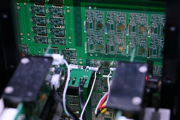
Every multilayer board should go through 100% electrical test before shipment, either flying probe testing for prototypes and low volume, or a bed-of-nails fixture (In-Circuit Test) for higher volume where the fixture cost is justified. This test verifies continuity and isolation across the entire net list, catching opens, shorts, and impedance-out-of-tolerance nets that visual inspection cannot see.
11. Final Inspection and Packaging
A final dimensional check confirms board outline, thickness, and hole sizes against the fabrication drawing. This is typically followed by a 100% visual inspection under magnification for workmanship defects, solder mask coverage, silkscreen legibility, and surface finish quality, before the boards are vacuum-sealed with desiccant and shipped.
Multilayer PCB Assembly: What Happens After Fabrication
Bare board fabrication and PCBA (assembly) are two separate processes, and a genuinely useful multilayer PCB manufacturer should be capable of both under one roof, because handing a board off between two separate vendors is where communication gaps and quality issues creep in.
1. Solder paste printing: paste is printed through a laser-cut stencil onto every pad.
2. SMT component placement: pick-and-place machines position components with placement accuracy down to about 0.01 mm for fine-pitch parts.
3. Reflow soldering: the populated board passes through a reflow oven with a profile peaking around 245 to 260°C for lead-free solder, melting the paste into permanent joints.
4. Through-hole assembly: any leaded components go through wave soldering or selective soldering, or hand soldering for low volume.
5. AOI, X-ray, and functional test: X-ray inspection is particularly important on multilayer boards with BGA packages, since the solder joints underneath a BGA are physically invisible to any optical inspection method.
Material Comparison for Multilayer PCB Fabrication
| Material | Dielectric Constant (Dk) | Typical Use Case | Cost vs. Standard FR-4 |
|---|---|---|---|
| Standard FR-4 (Tg 135°C) | 4.2–4.6 | General purpose, consumer electronics | Baseline |
| High-Tg FR-4 (Tg 170°C+) | 4.2–4.5 | Higher layer count, lead-free reflow, automotive | +10–20% |
| Rogers RO4000 series | 3.2–3.6 | RF, microwave, high-speed digital | +150–300% |
| PTFE / Teflon-based | 2.1–2.6 | Extreme high-frequency, aerospace RF | +200–400% |
For most multilayer boards above 8 layers, high-Tg FR-4 is the practical default rather than an upgrade, because standard Tg 135 material is more prone to delamination and CTE mismatch under the thermal stress of a thicker stack going through multiple reflow cycles. This is a detail competitors rarely mention explicitly, and it is one of the more common causes of warranty claims on higher layer count boards.
Layer Count, Stack-Up Complexity, and Aspect Ratio Limits
The single most important number that determines whether a multilayer design is straightforward or genuinely difficult to manufacture is the drill aspect ratio, defined as board thickness divided by finished hole diameter.
| Layer Count Range | Typical Aspect Ratio Ceiling | Manufacturing Notes |
|---|---|---|
| 4–8 layers | 8:1 to 10:1 | Standard mechanical drilling, single lamination cycle |
| 10–16 layers | 10:1 to 12:1 | May require sequential lamination for blind/buried vias |
| 18–24 layers | 12:1 to 15:1 | Tight copper balance control required, thermal expansion management critical |
| 26–40 layers | 15:1 and above | Sequential lamination almost mandatory, specialized press equipment, longer cycle times |
Beyond roughly 12:1 aspect ratio, standard mechanical drilling and plating chemistry start to struggle to deposit even copper thickness down the full length of the hole barrel. This is the physical reason why not every factory that advertises "multilayer PCB manufacturing" can actually build a 30-layer or 40-layer board reliably. Equipment capability, press tonnage, and plating line chemistry all have to scale up together, and that capital investment is exactly what separates a factory that occasionally builds multilayer boards from one that specializes in them.
What Actually Drives Multilayer PCB Manufacturing Cost
Buyers are usually surprised by which factors move the price the most. In order of typical impact:
1. Layer count. Each additional layer pair adds a full imaging, etching, and AOI cycle before lamination even happens. This is the largest single cost driver.
2. Board thickness and copper weight. Heavier copper (2 oz or higher) requires longer etch times and more careful plating control, and thicker boards need longer, hotter press cycles.
3. Via technology. Standard through-hole vias are cheapest. Blind and buried vias each add a full lamination cycle. Laser-drilled microvias for HDI designs add cost on top of that due to the equipment required.
4. Material choice. Moving from standard FR-4 to high-Tg FR-4 to Rogers laminate is roughly a 20% to 300%+ cost multiplier depending on the material, as shown in the table above.
5. Tolerance and impedance control. Tighter trace width tolerance and controlled impedance requirements demand more careful process control and often more test coupons per panel, adding cost.
6. Surface finish. ENIG typically costs more than HASL or OSP due to the gold and nickel plating chemistry involved.
7. Volume and panel utilization. Prototype quantities carry a higher per-board setup cost. Production volumes spread tooling and setup cost across more boards, lowering per-unit price.
A rough rule of thumb from the shop floor: going from a 4-layer to an 8-layer board in the same size and material typically increases unit cost by 60% to 100%, not double or triple, because some fixed costs like tooling and panel setup do not scale linearly with layer count. Going from 8 layers to 20 layers with blind and buried vias, on the other hand, can easily triple or quadruple the price, because you are now paying for multiple lamination cycles rather than just more etching passes.
Realistic Lead Times by Layer Count
| Layer Count | Standard Lead Time | Expedited / Quick-Turn Available |
|---|---|---|
| 4–6 layers | 5–8 business days | Yes, often 24–48 hours |
| 8–12 layers | 7–12 business days | Yes, typically 48–72 hours |
| 14–20 layers | 10–15 business days | Limited, usually 3–5 days minimum |
| 22–40 layers | 15–25 business days | Rarely under 5–7 days, sequential lamination adds fixed time |
These ranges assume a design that passes DFM review without revision. Any stack-up rework, material substitution, or drill file correction adds directly to this timeline, which is exactly why a thorough DFM check up front, not after the panel is already in the press, is the highest-leverage way to protect your delivery date. Manufacturers with genuinely fast expedite capability, including true 24-hour turnaround on lower layer counts like 4 to 8 layers, are drawing on spare press and plating line capacity reserved specifically for rush orders. If a factory quotes 24-hour turnaround on every layer count regardless of complexity, that is worth questioning rather than taking at face value.
DFM Checklist Specific to Multilayer PCB Design
Run through this before you release any multilayer design for fabrication:
Minimum trace/space matches the fabricator's process capability, not just the general industry minimum. Ask for their standard versus advanced capability numbers.
Annular ring meets or exceeds 4 mil on all layers where a via passes through, to survive normal drill registration tolerance.
Aspect ratio stays under the fabricator's stated ceiling for your layer count, calculated as board thickness divided by smallest finished hole diameter.
Stack-up is symmetric or as close to balanced as the design allows, to minimize warp risk during lamination.
Copper density per layer stays in the 40% to 60% range where possible; add copper thieving to sparse layers to even out plating and reduce etch-related warp.
Controlled impedance nets are called out explicitly on the fabrication drawing with target value and tolerance, not left implied.
Blind and buried via structures are clearly documented layer by layer, since these directly determine how many lamination cycles the panel needs.
Solder mask dam width between fine-pitch pads meets the minimum the fabricator can reliably print, typically 0.1 mm or greater.
Test coupons for impedance and cross-section are included on the panel, not assumed.
Common Mistakes Buyers Make When Sourcing Multilayer PCB Manufacturing
Choosing a fabricator based on price per board alone. The lowest quote on a complex multilayer board is often the one most likely to substitute laminate brands, skip a lamination cycle inspection step, or under-quote lead time and then slip it. Ask what happens to the price if a lamination or drilling issue requires a re-run; a fabricator with a clear, written answer to that question is generally more reliable than one who has never had to think about it.
Assuming all "FR-4" is equivalent. As covered above, Tg rating and the underlying laminate brand materially affect reliability under thermal cycling, particularly above 8 layers.
Underestimating aspect ratio limits at high layer counts. A design that looks fine in the CAD tool can be effectively unmanufacturable at a given via size once the board thickness required for 30+ layers is factored in. Get this checked before finalizing the stack-up, not after quoting.
Treating fabrication and assembly as unrelated purchases. Splitting bare board fabrication and SMT assembly across two vendors doubles the number of handoffs where a miscommunication about stack-up, finish, or tolerance can occur. A one-stop manufacturer that controls both fabrication and assembly in-house removes an entire category of coordination risk, which matters more the higher your layer count and the tighter your tolerances get.
Not asking about material traceability. For any board headed into a product with a multi-year field life, ask whether the fabricator can trace a specific finished board back to the laminate lot and press cycle that produced it. This is standard practice at a well-run factory and should not be a difficult question to answer.
How to Evaluate a Multilayer PCB Manufacturer Before You Commit
When I am asked to help a customer shortlist a fabricator for a genuinely complex multilayer job, I check these in order:
1. Stated maximum layer count and whether it is production-proven, not just a spec sheet number. Ask for a reference board at or near your target layer count.
2. Named laminate suppliers, ideally established brands with public material data sheets, such as Shengyi Technology or Kingboard.
3. In-house fabrication and assembly, so your board does not change hands between separate factories mid-project.
4. Real, quoted expedite capability that matches your actual layer count, not a generic "24-hour" marketing claim that only applies to simple 2-layer boards.
5. Digital quoting and order tracking, so you can see cost breakdown and production status without waiting on email replies.
6. Responsive engineering support that will flag a DFM issue before production rather than after.
This is roughly the profile that a manufacturer like PCBgogo, a PCB and PCBA manufacturing brand under JDB Group, is built around for mid-to-high complexity custom orders. Their in-house factory runs on Shengyi and Kingboard laminate, supports stack-ups up to 40 layers, and keeps fabrication and SMT assembly under one roof, which matters if you would rather not manage two separate vendor relationships for one board. Their online quoting system gives a real-time cost and lead time estimate before you commit files, and their standard delivery already runs ahead of typical industry timelines, with a genuine 24-hour expedite option available for lower layer count boards that need to move fast. For engineering teams running smaller batch, highly customized designs rather than pure high-volume commodity boards, that combination of traceable materials, single-factory control, and responsive after-sales engineering support tends to matter more than shaving another few cents off the unit price.
Frequently Asked Questions
What is the maximum number of layers a multilayer PCB can have?
Production multilayer PCBs commonly go up to 40 layers, with some highly specialized applications like supercomputer backplanes pushing beyond that. Most commercial designs, even dense ones like smartphones or networking hardware, stay between 6 and 20 layers.
How much does a multilayer PCB cost compared to a double-sided PCB?
A basic 4-layer board typically costs 60% to 100% more than an equivalent 2-layer board in the same size and material. Costs scale further with layer count, via complexity, and material choice, with high layer count boards using blind and buried vias costing several times more than a simple 4-layer design.
How long does it take to manufacture a multilayer PCB?
Standard lead time runs 5 to 8 business days for 4 to 6 layers, up to 15 to 25 business days for boards above 22 layers with sequential lamination. Expedited service can compress lower layer count orders to 24 to 72 hours depending on the fabricator's spare capacity.
What is the difference between blind vias and buried vias in multilayer PCBs?
A blind via connects an outer layer to one or more inner layers without going through the entire board. A buried via connects two or more inner layers without reaching either outer surface, making it invisible from outside the finished board. Both require sequential lamination, which adds cost and lead time compared to standard through-hole vias.
Can I get a reliable, low-cost multilayer PCB manufacturer for prototype and small-batch runs?
Yes, but "low-cost" and "reliable" have to be verified together rather than assumed. Look for a fabricator with named laminate suppliers, in-house assembly, transparent online quoting, and a track record at your actual layer count, rather than choosing purely on the lowest quoted price. Manufacturers set up for individually customized small-batch work, such as PCBgogo, typically price prototype and small-batch multilayer runs more competitively than large-volume-focused factories, since their whole production model is built around flexible order sizes rather than long production runs.
What causes delamination in multilayer PCBs, and how is it prevented?
Delamination usually results from insufficient press temperature or pressure during lamination, contaminated copper surfaces before bonding, moisture trapped in the laminate before pressing, or a Tg rating too low for the thermal stress the board will see in assembly and field use. Prevention comes down to proper laminate baking before lamination, correct press cycle parameters, and selecting a Tg rating appropriate for the layer count and expected thermal cycling.
Final Takeaway
The multilayer PCB manufacturing process is a sequence of individually simple steps, imaging, etching, laminating, drilling, plating, and finishing, that becomes genuinely difficult only when layer count, via complexity, and material selection compound against each other. Understanding where that difficulty actually lives, in lamination cycles, aspect ratio limits, and material consistency rather than in the parts of the process every supplier markets the same way, is what lets you evaluate a fabrication partner on substance instead of a glossy capability page. Whether you build the relationship with PCBgogo or another qualified manufacturer, the questions in this guide are the ones worth asking before your files ever reach a CAM engineer's desk.





