
 日本語
日本語

QUICK ANSWER Identify the power input and ground, divide the drawing into functional blocks, and trace one important signal from source to destination. Read each component's reference designator, value, pin number, and net label as you go. Check the datasheet whenever an IC or unfamiliar symbol determines how a block works.
A schematic is a circuit's logical map. It shows which component pins are electrically connected, not where the parts sit on the finished PCB. Once you understand that distinction, even a crowded circuit diagram becomes easier to approach.
This guide explains how to read schematic diagrams in seven repeatable steps. You will learn the essential symbols, reference designators, nets, power rails, and signal-flow conventions, then use them to interpret and troubleshoot a simple circuit.
Quick Answer: How Do You Read a Schematic?
That method is more useful than trying to memorize every electronic symbol before opening a real schematic.
What a Schematic Shows—and What It Does Not
A schematic describes electrical intent. Symbols represent components, while lines or matching net labels represent connections. It helps designers review a circuit, generate a netlist, create a PCB layout, and diagnose faults.
It is not a physical map. Two parts drawn side by side may be far apart on the board. Package size, orientation, trace width, layer changes, and placement belong to the PCB layout and assembly documents.
Think of a schematic as a subway map: it prioritizes connections and function over physical distance.
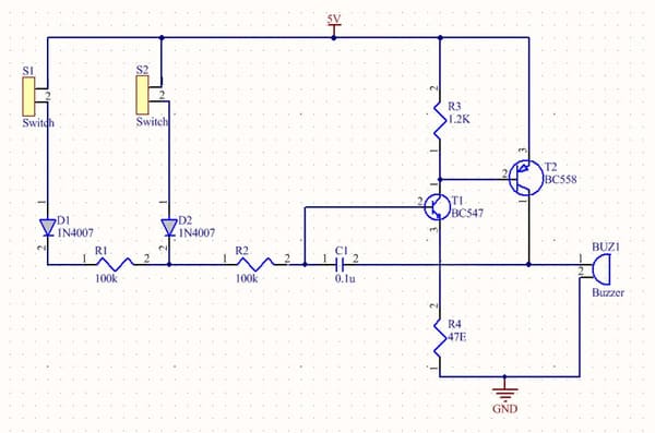
Learn the Basic Schematic Symbols
You do not need to memorize a complete symbol library. Begin with the parts that appear in most circuits:
| Component | Common designator | What to look for |
|---|---|---|
| Resistor | R | Zigzag or rectangle; value such as 1 kΩ or 10 kΩ |
| Capacitor | C | Two plates; a + or curved plate may indicate polarity |
| Inductor | L | A series of loops or curved sections |
| Diode or LED | D | A diode bar shows polarity; LED arrows point outward |
| Transistor or MOSFET | Q | Three or more pins labeled by function |
| Integrated circuit | U | Box with numbered or named pins |
| Connector | J or P | Numbered contacts that link the board to other hardware |
| Switch | S or SW | Contacts show which nodes connect in each position |
| Fuse | F | Protective device placed in a current path |
| Crystal or oscillator | Y | Timing component, often near a microcontroller |
Symbol styles vary between IEC and ANSI conventions, so use the designator and value as clues. For an unfamiliar IC such as U3, the part number and datasheet explain what its pins do.
Understand Nets, Junctions, and Labels
The lines between symbols are nets: electrical connections later implemented as PCB traces, planes, wires, or cable conductors.
A solid dot where lines meet normally indicates a connected junction.
Lines that cross without a dot normally do not connect.
A bridge or "hop" over another line also indicates no connection.
Matching net labels connect points without a continuous line across the page.
A bus groups related signals; each member still has its own name.
On an old scan, a junction dot can disappear. Confirm ambiguous connections using net names, pin functions, or the original design file.
Power symbols are named nets. Every +3V3 symbol in the same scope usually refers to the same rail. However, GND, AGND, DGND, protective earth, and chassis ground may be separate networks. Never assume every ground symbol is interchangeable.
Read Reference Designators, Values, and Pin Numbers
A reference designator uniquely identifies a component. In R7 10 kΩ, R7 identifies the resistor and 10 kΩ gives its value. The same designator should appear in the BOM, PCB layout, assembly drawing, and often on the silkscreen.
An IC symbol may arrange pins by function rather than physical order. Pin 1 on the drawing must still map to pin 1 on the footprint. Polarized capacitors, diodes, LEDs, and many connectors must also match the specified orientation.
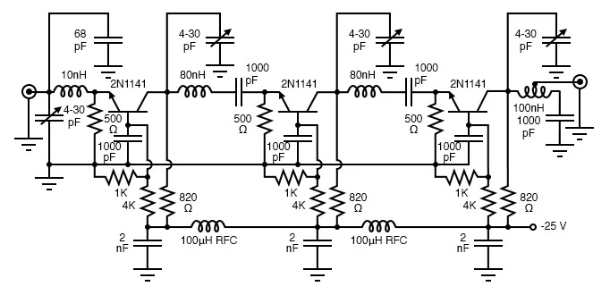
How to Read a Schematic in 7 Steps
1. Check the title, revision, and notes
Confirm the drawing and revision. Read notes about supply voltage, optional or unpopulated parts, test points, and default ratings. An obsolete revision can lead to the wrong repair or build decision.
2. Find the power path and grounds
Locate the power source, input protection, regulator, switches, and rails such as VIN, +5V, and +3V3. Follow each rail to the active components it supplies and identify the relevant ground.
3. Divide the circuit into functional blocks
Break the drawing into small subsystems such as:
input protection and power conversion;
a microcontroller or processor;
sensors and analog conditioning;
communications such as USB, UART, I2C, or SPI;
output drivers for LEDs, relays, motors, or speakers.
Read one block at a time, then note the nets connecting it to the next block.
4. Trace one signal from source to destination
Choose the signal most closely related to the circuit's purpose. On a sensor board, for example, follow the sensor output to the processor. Inputs often appear on the left and outputs on the right, but this is a convention, not a rule. Feedback and multi-page designs may flow differently.
5. Identify the main active component
The main IC often explains the surrounding parts. Read its part number, pin names, supply requirements, and functional diagram in the datasheet. A net entering an op-amp input, regulator feedback pin, or microcontroller communication pin reveals its context.
6. Ask why each supporting part is there
Determine what each supporting part does. A resistor may limit current, pull up an input, set gain, or divide voltage. A capacitor may decouple a supply, couple an AC signal, filter noise, or set timing. Connections and value reveal the likely role.
7. Cross-check the schematic against the PCB and BOM
Use the reference designator to find the physical part. Verify that the BOM part number, schematic value, footprint, and assembly orientation agree. EDA cross-probing helps, but manual checks remain useful during revision reviews.
Worked Example: Reading a Simple LED Circuit
Imagine a 5 V supply connected to R1, then to LED D1, and finally to GND.
The 5 V symbol identifies the source rail.
R1 1 kΩlimits the current through the LED.D1must be oriented with the correct anode and cathode.The ground symbol completes the path.
If the LED's forward voltage is approximately 2 V, the resistor sees about 3 V. Ohm's law gives an estimated current of 3 V ÷ 1,000 Ω = 3 mA. The exact result depends on the LED and supply tolerances, so the component datasheet remains the authority.
If the LED is dark, verify the 5 V rail, measure both sides of R1, confirm D1 polarity, and check its ground path.
Common Mistakes When Reading Circuit Diagrams
Treating the schematic as a placement drawing: electrical proximity does not guarantee physical proximity.
Missing a named connection: matching labels may join distant pages without a visible wire.
Assuming every crossing connects: look for a junction dot and confirm ambiguous scans.
Ignoring polarity or pin numbers: the right component in the wrong orientation can still fail.
Reading values carelessly:
4R7means 4.7 Ω, while4K7means 4.7 kΩ.Assuming all grounds are identical: analog, digital, chassis, and earth grounds may serve different purposes.
Trying to understand everything at once: begin with one block and one path.
From Schematic to a Manufacturable PCB
A verified schematic proves the circuit works electrically, but it is not something a factory can build from. Two more steps stand between the schematic and a physical board: turning the completed layout into manufacturing data, and then running that data through actual fabrication.
The first step happens after layout and routing are finished. Run a design rules check on the finished layout, then export the manufacturing package, meaning Gerber files for each copper, solder mask, and silkscreen layer, plus the drill file, following the schematic-to-Gerber workflow. This is also where schematic-stage mistakes tend to surface: a pin that was never actually wired to the net it looks connected to on paper will show up as a broken trace in the exported files.
Before treating that export as final, load it into a Gerber viewer rather than trusting the output blindly. PCBgogo's own Gerber Viewer opens Gerber and drill files directly in the browser, so you can confirm every copper layer, hole, and outline matches the design before the files go anywhere near a factory.
Turning the Files Into an Actual Board
Verified manufacturing data still needs to go through fabrication before it becomes a board you can hold. PCBgogo's core business is exactly this step: taking uploaded Gerber, drill, and BOM files and turning them into fabricated and, where needed, assembled PCBs.
Every order submitted to PCBgogo is reviewed by an engineer before production starts, catching file or manufacturability issues before they reach the fabrication floor rather than after. For boards that also need components populated, PCBgogo's turnkey assembly service sources the parts, places and solders them, and returns a finished, tested board instead of a bare one.
For assembly specifically, the schematic and Gerber files are not the complete package. A working handoff still needs the BOM, a pick-and-place (centroid) file, an assembly drawing, and polarity notes, all kept on the same revision as the schematic so nothing gets built against outdated data.
Frequently Asked Questions
Where should I start on a complex schematic?
Begin with the title and power rails, divide the design into blocks, and choose the signal related to the function you want to understand. Use net labels to follow that signal across sheets.
What is the difference between a schematic and a wiring diagram?
A schematic emphasizes electrical function and logical connections. A wiring diagram focuses more on physical wires, connectors, terminal numbers, and installation details. A PCB layout shows the actual component placement and copper routing.
Can a schematic tell me where a component is on a PCB?
Not by position. Use its reference designator—such as R12 or U3—to locate the matching part in the PCB layout, assembly drawing, or silkscreen.





