
 日本語
日本語

If you've ever debugged a TIA at midnight wondering why the output looks like a radio broadcast, you're in the right place. Photodiode signals are small, noise is everywhere, and a sloppy PCB layout can undo a carefully designed circuit before it ever gets tested. This guide covers everything from basic principles to layout-level design decisions, helping you build a stable photodiode transimpedance amplifier that performs reliably in real-world circuit conditions.
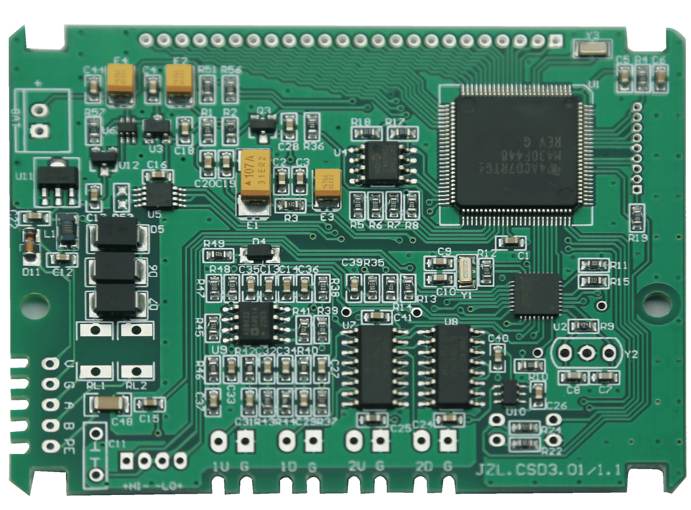
What Is a Transimpedance Amplifier?
A transimpedance amplifier (TIA) is a current-to-voltage converter. It takes a tiny input current — typically from a photodiode, but also from photomultiplier tubes, ion detectors, or current-output DACs — and converts it into a proportional voltage that downstream circuitry can actually work with.
The core relationship is simple:
V_out = I_in × R_f
Where R_f is the feedback resistor. For example, a photodiode producing 1 μA of current through a 1 MΩ feedback resistor will generate a 1 V output. The op-amp’s inverting input is held at a virtual ground, which keeps the photodiode’s cathode at a stable bias even as the output changes. This stability is important because it helps maintain linear diode operation and reduces variations in junction capacitance.
What makes TIA design non-trivial is that R_f and the parasitic capacitances at the input node interact to form a pole that can push the circuit into oscillation. That's the central challenge this guide addresses.
Transimpedance Amplifier Applications
TIAs show up wherever you need to convert small photocurrents or charge-based signals into usable voltages. Common use cases include:
Optical communications — fiber receivers, LiDAR return signal detection, free-space optical links
Analytical instruments — spectrophotometers, fluorescence detectors, flow cytometers
Medical imaging — CT detector arrays, pulse oximetry front ends, PET scanners
Industrial sensing — laser rangefinders, smoke detectors, barcode scanners
AI and autonomous systems — ToF depth sensors for robotics and ADAS, structured light 3D cameras
Scientific research — single-photon counting front ends, lock-in amplifier inputs
In virtually all of these, the signal chain starts with a TIA. Getting it right sets the noise floor for everything downstream — and how well that carries through to the final board depends heavily on how optoelectronic PCBAs are manufactured and assembled.
How a Transimpedance Amplifier Circuit Actually Works
A minimal transimpedance amplifier circuit has three components: an op-amp, a feedback resistor R_f, and a feedback capacitor C_f. Here's what each does and why it matters.
The op-amp needs a low input bias current (to avoid adding a DC offset equal to I_bias × R_f), sufficient gain-bandwidth product, and low voltage noise. For precision DC applications, choose a FET-input op-amp like the OPA128 or LTC6268. For high-speed work, look at the OPA657 or THS3201.
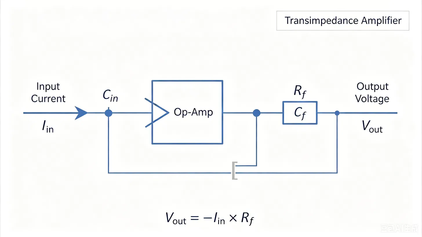
R_f sets the transimpedance gain. Larger values give more signal but introduce more Johnson noise (V_n = √(4kTR_f·BW)) and push the –3dB bandwidth lower.
C_f is placed in parallel with R_f. This is not optional — it compensates for the pole created by R_f and the total input capacitance C_in (diode junction capacitance + op-amp input capacitance + PCB stray capacitance). Without C_f, the phase margin collapses and the output rings or oscillates.
The stability criterion gives you a starting point for C_f:
C_f ≥ √(C_in / (2π × R_f × GBW))
Run a SPICE simulation after calculating C_f. Real-world parasitics always add margin you didn't budget for.
Low Noise Transimpedance Amplifier Design
For any application where sensitivity matters — single-photon work, trace chemical detection, low-light imaging — low noise transimpedance amplifier design requires thinking about three distinct noise sources simultaneously.
1. Johnson noise from R_f This is often the dominant term at low frequencies. It's unavoidable for a given R_f, but you can narrow bandwidth with a smaller C_f or a post-amplifier filter to reduce integrated noise.
2. Op-amp current noise (I_n) Each nanoamp of input current noise generates I_n × R_f of output noise. This is why FET-input op-amps — with their femtoamp-level input current noise — are standard for low noise transimpedance amplifier designs. BJT-input op-amps have superior voltage noise but typically far worse current noise.
3. Op-amp voltage noise (e_n) The voltage noise sees a noise gain of (1 + C_in/C_f) at high frequencies, which can become the dominant noise source if C_in is large and C_f is small. Keep C_f as large as stability allows, and minimize C_in by placing the op-amp physically close to the photodiode.
A practical design exercise: if you're targeting a noise equivalent power (NEP) of 1 pW/√Hz at 850 nm with a Si photodiode (responsivity ~0.5 A/W), you need an input-referred current noise floor below 0.5 fA/√Hz. That immediately rules out most general-purpose op-amps and most BJT-input parts.
How PCB Layout Makes or Breaks Your TIA Design
You can have a textbook-perfect schematic and still get a noisy, unstable board if the transimpedance amplifier PCB layout is wrong. These are the layout rules that actually matter:
1. Guard rings: Draw a copper ring around the inverting input node (–IN, R_f, C_f, and the photodiode anode) and connect it to the output or to a driven shield at the same potential. This eliminates leakage currents from the PCB surface — which at 10^13 Ω surface resistance can add picoamp-level leakage directly into your signal node. For femtoamp-level work, consider Teflon standoff connectors for the photodiode lead instead of standard PCB pads.
2. Minimize stray capacitance at the inverting input: Every extra picofarad of C_in degrades phase margin and raises high-frequency noise gain. Keep copper away from the inverting input node. Use a ground plane cutout directly beneath the –IN pin of the op-amp.
3. Decoupling: Place 100 nF ceramic caps as close as possible to the op-amp supply pins — within 2–3 mm if possible. Add a 10 μF bulk cap nearby. Poor supply bypassing couples supply noise into the output.
Separate analog and digital grounds: If your board has a mixed-signal design, keep the TIA on the analog section. Route digital signals away from the input node and the feedback network.
4. Short feedback path: R_f and C_f should be as close to the op-amp pins as possible. Long traces add inductance and pick up interference.
For high-speed TIA designs (>10 MHz bandwidth), pay attention to trace impedance and avoid vias in the signal path where possible.
FAQ
Q: What's the difference between a TIA and a regular inverting amplifier?
A: A standard inverting amplifier converts voltage to voltage. A TIA converts current to voltage — the input impedance is near zero (virtual ground), which is exactly what a photodiode needs for linear operation. The gain is set by R_f alone, not a resistor ratio.
Q: Why does my TIA oscillate?
A: Almost always a stability problem caused by insufficient C_f. The parasitic capacitance at the inverting input (from the photodiode, PCB traces, and op-amp input) forms a pole with R_f that reduces phase margin. Calculate your required C_f using the stability formula, then verify in SPICE. Also check for inadequate supply bypassing.
Q: How do I choose between a FET-input and BJT-input op-amp for my TIA?
A: It depends on your noise budget and bandwidth. FET-input op-amps have very low current noise (femtoamps), making them better for high-impedance, low-bandwidth applications. BJT-input op-amps have lower voltage noise and are often preferred for wide-bandwidth TIAs where the voltage noise term dominates. When in doubt, simulate both with realistic noise models.
Q: What value should I use for C_f?
A: Use the stability formula as a starting point: C_f ≥ √(C_in / (2π × R_f × GBW)). This gives approximately 45° of phase margin. For real-world margin, add 20–30% and verify with simulation. Measure the actual step response on your first prototype before committing to a value.
Q: How does PCB layout affect TIA noise?
A: Significantly. Surface leakage currents on FR4 can inject picoamps directly into the input node, swamping femtoamp-level signal currents. Guard rings driven at the output potential eliminate this path. Stray capacitance from copper pours near the –IN node increases C_in, raises noise gain, and reduces phase margin. A careful layout can easily mean a 10× improvement in practical noise performance compared to a careless one.
Q: Can I use a transimpedance amplifier for non-optical applications?
A: Absolutely. Any application requiring current-to-voltage conversion — ionization chambers, electrochemical sensors, MEMS accelerometers with capacitive readout, or current-output DAC buffering — can use a TIA front end. The design principles are identical regardless of the current source.





