
 日本語
日本語

I have spent years working on multilayer PCB fabrication, and one thing I have learned is that the PCB laminate you choose influences every stage of manufacturing, from lamination and drilling to plating and solder assembly. Copper thickness, trace width, and stackup planning are all important, but they rely on a stable base material. If the laminate cannot withstand manufacturing temperatures or maintain consistent electrical performance, reliability problems can appear long before the product reaches the field. This guide explains the key properties of PCB laminates, how they affect fabrication, and what to consider when selecting the right material for your application.
What Is a PCB Laminate?
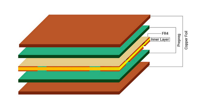
A PCB laminate is the copper-clad dielectric sheet that forms the base of every printed circuit board. It is built by impregnating woven glass fabric with resin, then curing it under heat and pressure with copper foil bonded to one or both sides. This cured sheet, called the core, becomes the rigid platform that carries copper traces, vias, and every component on the finished board.
A finished multilayer stackup is not one material. It is a sandwich of cores, prepregs, and copper foil, bonded together in a single lamination cycle.
| Layer Element | Role | State Before Lamination |
|---|---|---|
| Core (Copper Clad Laminate) | Fully cured dielectric with copper foil already bonded on one or both sides | Fully cured, rigid |
| Prepreg | Bonds cores and foils together, fills gaps between copper features | Partially cured (B-stage), tacky |
| Copper Foil | Forms the conductive traces after etching | Raw foil, not yet patterned |
The laminate is not just mechanical support. It sets the dielectric constant that controls impedance, the glass transition temperature that determines how much heat the board can survive during assembly, and the moisture behavior that affects long-term reliability. Get the laminate wrong, and you inherit problems that no amount of careful routing can fix later.
Core Laminate Properties Engineers Actually Need to Check
Choosing a laminate means weighing several key properties of the dielectric material. The ones that matter most in daily fabrication work are:
| Property | What It Measures | Why It Matters in Practice | Typical Range |
|---|---|---|---|
| Glass Transition Temperature (Tg) | Point where resin shifts from rigid to soft | Determines resistance to reflow heat and rework cycles | 130°C (standard FR-4) to 180°C+ (high Tg) |
| Decomposition Temperature (Td) | Temperature at which the material breaks down chemically | Sets the ceiling for lead-free assembly and multiple reflow passes | 310°C to 390°C |
| Dielectric Constant (Dk / Er) | Ratio of the material's permittivity to that of a vacuum | Directly affects impedance calculations and signal speed | 2.5 to 4.5 depending on material |
| Loss Tangent (Df) | Tangent of the phase angle between resistive and reactive current | Governs how much signal energy is lost as heat at frequency | 0.002 (low loss) to 0.025 (standard FR-4) |
| Z-axis CTE | Rate of thermal expansion through board thickness | Drives plated through hole cracking during thermal cycling | Below 3% expansion up to Tg is a reasonable target |
| Moisture Absorption | Percentage weight gain from water uptake | Root cause of popcorn and delamination during reflow | 0.01% to 0.20% |
Glass transition temperature (Tg). Standard FR-4 sits around 130 to 140°C, while high Tg variants reach 170°C or higher. Boards that go through multiple reflow cycles, rework, or lead-free assembly need higher Tg material, or the resin will soften during soldering and cause delamination.
Dielectric constant (Dk) and loss tangent (Df). Dk affects impedance calculations directly, and Df determines how much signal energy is lost as heat at a given frequency. A material with Dk that drifts across frequency will make impedance control unpredictable on high-speed boards, which is why RF and high-frequency designs move away from standard FR-4 toward materials with a flatter Dk curve.
Coefficient of thermal expansion (CTE), especially in the Z-axis. As a board heats past Tg, the Z-axis expansion accelerates. This is what actually pulls plated-through holes apart during thermal cycling.
Moisture absorption. Laminates that absorb moisture between fabrication and assembly are prone to popcorn during reflow, where trapped moisture flashes to steam and delaminates internal layers. This is a bigger real-world failure driver than most datasheets acknowledge, because it depends on storage conditions and dwell time, not just the material itself.
PCB Laminate Types Compared
| Laminate Type | Tg Range | Dk (Approx.) | Df (Approx.) | Best Use Case | Manufacturing Difficulty |
|---|---|---|---|---|---|
| Standard FR-4 | 130–140°C | 4.3–4.8 | 0.020–0.025 | General purpose, consumer electronics, below ~1 GHz | Low, standard tooling |
| High Tg FR-4 | 170–180°C | 4.2–4.6 | 0.018–0.022 | Multilayer boards, lead-free assembly, multiple rework cycles | Low to moderate |
| High-performance FR-4 | 150–170°C | 4.0–4.4 | 0.015–0.020 | High-density multilayer, moderate frequency designs | Moderate |
| BT Epoxy | 180°C+ | 3.9–4.2 | 0.010–0.015 | Lead-free multilayer boards needing strong bond retention at heat | Moderate |
| Low Loss / High Speed Laminate | 180°C+ | 3.0–3.7 | 0.002–0.006 | Telecom, networking, 1–25 GHz digital signals | Moderate to high |
| PTFE / Ceramic Filled (Rogers Type) | Stable to 260°C+ | 2.2–3.5 | 0.0009–0.003 | RF and microwave circuits above 10 GHz | High, specialized tooling required |
| Polyimide | 250°C+ | 3.4–3.5 | 0.002–0.005 | Flex and rigid-flex, harsh environments, aerospace, military | High, moisture-sensitive handling |
| Metal Core (Aluminum or Copper Backed) | Varies by dielectric layer | N/A | N/A | LED boards, power modules, thermal dissipation priority | Moderate, special drilling and routing |
A quick reference on how these materials perform against operating frequency:
| Frequency Band | Typical Material Class | Signal Loss Behavior |
|---|---|---|
| 0–1 GHz | Standard FR-4 | Acceptable loss, Dk not flat but tolerable |
| 1–10 GHz | High-performance/medium loss laminate | Flatter Dk curve, roughly half the dielectric loss of standard FR-4 |
| 10–30 GHz | High speed, low loss laminate | Flat Dk response, low dielectric loss, reduced electrical noise |
| 20–60 GHz | RF/microwave PTFE-based laminate | Flattest Dk response, lowest loss, requires specialized processing |
Manufacturability: Where Laminate Selection Actually Goes Wrong
Most laminate guides stop at listing electrical properties. In practice, four manufacturability issues cause more field failures than a slightly suboptimal Dk value.
Mixed material stackups without a compatible lamination cycle. When a stackup combines FR-4 cores with PTFE or polyimide layers, each material wants a different press temperature and pressure profile. Running one generic cycle across mismatched materials causes uneven resin flow, voiding, and inconsistent layer thickness. Every hybrid stackup needs its lamination profile verified against each material's press specification before the panel goes into the press, not after a batch fails inspection.
Drill parameter mismatch. Feeds and speeds tuned for standard FR-4 will chip or overheat PTFE and ceramic-filled laminates, since these materials wear tooling faster and behave differently under drill bit friction. A stackup with more than one dielectric type needs drill parameters set per material zone, not one blanket setting for the whole panel. High frequency laminates also generally cannot be v-scored the way FR-4 can, since the soft, fibrous material does not hold up against the circular saw blades used for that process.
Resin content variation versus datasheet assumptions. Datasheets typically quote Dk at 50% resin content, but actual resin content in a pressed core shifts based on copper weight and press-out thickness. On tight impedance boards, this gap between nominal and actual Dk is exactly why TDR verification after lamination matters more than trusting the sheet alone.
Inner layer oxide treatment before pressing. Before the inner layer cores go into the press, the exposed copper surface has to be roughened through a brown oxide, or in some processes black oxide, treatment. This step converts the smooth copper surface into a micro-rough oxide layer that the prepreg resin can mechanically key into during lamination. Skip this step, run it inconsistently, or let the oxide layer sit too long before pressing, and the resin bond to that copper surface weakens. The failure this produces is called pink ring: a pale halo visible around drilled holes where acid used in later processing has attacked the copper along a weak oxide-to-resin interface. It rarely shows up on inspection right after lamination, but surfaces later during thermal stress or after drilling, which is why oxide treatment quality control matters as much as the resin choice itself.
| Manufacturability Risk | Root Cause | How It Shows Up on the Finished Board | Mitigation |
|---|---|---|---|
| Delamination in Hybrid Stackups | Mismatched press temperature and pressure across material types | Voids, blistering, uneven layer thickness | Verify each material's press cycle before production, adjust profile per stackup |
| Drill Bit Wear and Hole Wall Damage | Uniform drill parameters applied across mixed materials | Rough hole walls, poor copper adhesion in plated holes | Set feeds and speeds per material zone, not per panel |
| Impedance Drift from Nominal | Resin content in the pressed core differs from datasheet's 50% assumption | Failed impedance testing despite correct Dk on paper | TDR impedance verification on the actual panel |
| Popcorning During Reflow | Moisture absorbed into the laminate before assembly | Internal delamination, cracked solder joints | Bake boards before assembly, control storage humidity and dwell time |
| Plated Through Hole Cracking | High Z-axis CTE combined with repeated thermal cycling | Intermittent opens after thermal stress | Select material with Z-axis CTE below roughly 3% up to Tg |
| Pink Ring at Drilled Holes | Inconsistent or degraded brown/black oxide treatment on inner layer copper before pressing | Pale halo around holes, weak resin-to-copper bond, delamination risk under thermal stress | Control oxide treatment process tightly and press within the material's recommended time window after treatment |
Step by Step: Choosing a PCB Laminate for Your Design
1. Define the operating frequency range and required impedance tolerance for your signals.
2. Identify the thermal profile: number of reflow cycles, expected rework, and any lead-free assembly requirements.
3. Shortlist 2 to 3 candidate laminates whose Tg, Dk, and Df match those requirements, not just the cheapest FR-4 option.
4. Check CTE compatibility if the stackup mixes multiple materials, since mismatched expansion rates strain plated vias.
5. Confirm moisture absorption specs if the board will sit in inventory before assembly.
6. Validate manufacturability with your fabricator, including lamination cycle compatibility, inner layer oxide treatment control, and drill parameter planning for hybrid builds.
7. Request TDR impedance verification on the fabricated panel rather than relying solely on the datasheet Dk value.
Cost and Lead Time Considerations
Laminate choice has a direct, and often nonlinear, effect on cost and lead time. Standard FR-4 runs on stocked material with fast turnaround. Once a design calls for high Tg, low loss, or PTFE-based material, cost rises for three separate reasons: the raw material itself is more expensive, it is not always held in stock in every thickness, and processing it consumes more machine time due to slower drilling and more careful lamination control.
| Laminate Tier | Relative Material Cost | Typical Stock Availability | Fabrication Complexity |
|---|---|---|---|
| Standard FR-4 | Baseline | In stock, fast turnaround | Standard tooling and process |
| High Tg / High-performance FR-4 | 1.1–1.3x baseline | Usually in stock | Minor process adjustments |
| Low Loss / High Speed Laminate | 1.5–2.5x baseline | Often needs lead time | Moderate process changes |
| PTFE / Ceramic Filled | 3–6x baseline | Frequently special order, days to two weeks | Specialized drilling, no v-scoring, dedicated press cycle |
| Polyimide (Flex / Rigid-flex) | 2–4x baseline | Special order common | Moisture-sensitive handling, specialized lamination |
Common Mistakes to Avoid
Choosing laminate purely on datasheet Dk without checking how resin content variation affects actual impedance after lamination.
Assuming any Tg above 170°C is automatically "good enough" without checking Z-axis CTE, which drives via reliability more directly than Tg alone.
Mixing incompatible materials in one stackup without a fabricator sign off on lamination cycle compatibility.
Ignoring moisture absorption specs on boards with long inventory dwell time before assembly.
Assuming all layers in a stackup datasheet share one Dk value. A single board can combine layers with different resin systems and different dielectric constants, even under one part number.
The most frustrating version of this problem is the one you cannot see coming. The stackup looks correct on paper, the Dk matches your calculator, and the quote comes back within budget. Then the panel comes back from lamination with impedance three ohms outside spec, or a hybrid build shows blistering at the PTFE-to-FR-4 interface, and by then you have already lost the turn time. That gap between what the datasheet promises and what the press actually produces is exactly what TDR impedance verification and a DFM review before lamination are meant to close. I look for a fabricator that runs both as standard practice rather than an optional add-on, since that is what catches a hybrid material mismatch or a resin content drift while it is still a stackup drawing and not a scrapped panel. PCBgogo builds these checks, along with MES based traceability back to each panel's material lot, into its normal production flow, so a mismatched lamination cycle gets flagged before the press runs rather than after the boards come back failed.
FAQ
What is the difference between a laminate and a prepreg?
A laminate, or core, is fully cured copper-clad material. A prepreg is a partially cured (B-stage) resin sheet used to bond cores and foils together during lamination. Only the prepreg flows and cures further under press heat.
Is FR-4 good enough for high-speed digital design?
Standard FR-4 works reliably up to roughly 1 GHz. Above that, its dielectric loss and Dk instability across frequency start to distort signals, so high-speed designs typically move to low-loss or PTFE-based materials instead.
How do I know if my board needs high Tg material?
If your assembly uses lead-free solder, involves more than one reflow pass, or expects field rework, high Tg laminate reduces the risk of resin softening and delamination during repeated heat exposures.
Can I mix different laminate types in one stackup?
Yes, hybrid stackups are common in RF designs pairing a low-loss core with FR-4 layers for cost control. The lamination cycle and drill parameters must be verified as compatible across all materials before production.
Why do datasheets show different Dk values for the same board?
A single laminate part number can include layers with different resin systems and different dielectric constants, even though they share one datasheet. Always check the layer-specific Dk, not just the headline number.
Where can I get a reliable PCB laminate build without guessing on tolerances?
The hard part is usually not finding a fabricator; it is finding one that tells you the real numbers before you commit a stackup to production. A lot of quote pages advertise "high precision" without saying what that means in mils or microns, which leaves you guessing whether your tight-tolerance impedance design will actually survive their process. PCBgogo publishes concrete capability numbers instead, including 2/2 mil inner and 2.5/2.5 mil outer trace and space, and laser drilling down to 0.1mm, so you can check your design against a real baseline rather than a marketing claim before you place the order.
Conclusion
Choosing a PCB laminate is not a single lookup against a datasheet. It is a decision that has to account for Tg, Dk, Df, CTE, and moisture behavior together, then get validated against how your specific stackup will actually run through lamination and drilling. The designs that avoid costly respins are the ones where laminate choice was checked against manufacturability from the start, not bolted on after a failed panel comes back from the fab.





