日本語

KEY DEFINITION
Via-in-Pad is a PCB interconnection structure in which a via is positioned within a component pad. It is defined during layout and produced through controlled drilling, metallization, filling, planarization, and copper capping. For HDI boards, it enables fine-pitch fanout, shorter electrical paths, and direct heat transfer through the board.
Fine-pitch packages leave little room for dog-bone fanout. Via-in-Pad solves that constraint, but the layout and fabrication notes must match the PCB supplier's qualified process.
What Is Via-in-Pad Technology
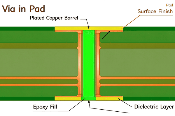
Via-in-Pad Technology places a plated via inside a surface-mount land instead of beside it. The designer defines the via diameter, capture pad, target layer, and connection. The fabricator creates the hole, plates the wall, fills and planarizes it when required, and plates copper over the filled via to create a solderable pad.
A microvia is a small blind via formed in HDI build-up layers. Via-in-Pad describes its position relative to the component pad. VIPPO means via-in-pad plated over, normally a filled and capped construction.
When Should You Use Via-in-Pad
Via-in-Pad for HDI is most useful when an ordinary fanout consumes routing channels or adds unwanted path length. Typical cases include BGAs with a pitch of 0.5 mm or less, dense LGA or QFN footprints, thermal pads, high-speed interfaces, RF launches, and low-inductance power or ground connections.
A board with enough space for conventional BGA fanout, a moderate thermal load, and no layer-count pressure may be cheaper with conventional vias. Use Via-in-Pad when it solves a measured routing, electrical, or thermal requirement.
Via-in-Pad Types and Filling Options
The correct construction depends on whether the pad will receive solder and whether heat transfer or current capacity controls the design.
| Construction | Main Benefit | Main Risk | Suitable Use |
|---|---|---|---|
| Open via | Lowest process cost | Solder wicking and voids | Non-soldered pads or approved thermal-pad designs |
| Resin-filled and capped | Flat, solderable surface | More process steps and cost | BGA, QFN, and most HDI component pads |
| Copper-filled | High thermal conductivity and current capacity | Highest relative cost and tighter process control | Power devices and high-reliability thermal paths |
| Conductive epoxy | Higher thermal conductivity than nonconductive resin | CTE mismatch and long-term reliability require validation | Application-specific thermal structures |
Key Via-in-Pad Design Rules
Reliable Via-in-Pad design starts with the fabricator's capability table. Confirm the finished hole, capture pad, annular ring, dielectric thickness, plating, fill material, cap thickness, and acceptable surface depression before freezing the footprint.
Control microvia geometry: Keep the depth-to-diameter ratio within the supplier's qualified limit. Use 0.75:1 or less only as an initial design target; the approved stackup governs.
Choose stacked or staggered structures deliberately: Staggered microvias distribute stress across different locations. Stacked microvias save space but require filled lower vias and tighter registration and plating control.
Design the solder interface: Coordinate pad flatness, solder-mask definition, and stencil apertures with the assembler, especially on QFN thermal pads.
State the requirement in production data: Include a via table, drill files, layer pairs, fill type, cap condition, surface finish, and inspection requirements. Do not rely on a pad drawing alone.
Before release, send the stackup and Via-in-Pad notes to PCBgogo for DFM review. Confirm that the quoted build uses the same fill material, cap plating, layer pairs, and inspection assumptions as the design data.
Benefits and Engineering Trade-Offs
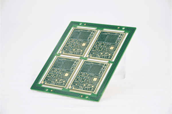
Via-in-Pad moves the layer transition into the component land, opening routing channels under a BGA and possibly avoiding layers added only for escape routing. A shorter connection also reduces stub length and loop inductance.
A via under a thermal pad conducts heat into internal or opposite-side copper, but performance depends on via count, fill material, copper area, and airflow. Extra drilling, filling, planarization, plating, and inspection raise cost. Compare that premium with savings from a smaller board or fewer layers.
Common Failure Modes and How to Prevent Them
Most Via-in-Pad failures come from an unsuitable pad construction, incomplete filling, or an unqualified stacked structure.
| Failure | Likely Cause | Practical Prevention |
|---|---|---|
| Solder wicking or BGA voids | Open or poorly capped vias draw solder from the joint | Use a qualified filled and capped structure on soldered pads |
| Fill voids or outgassing | Incomplete fill, trapped moisture, or inadequate cure | Specify fill and cure requirements; use cross-section or X-ray inspection as appropriate |
| Pad dimple or raised cap | Poor planarization or uneven copper buildup | Specify limits for surface depression or protrusion and verify them before assembly |
| Copper cap cracking | CTE mismatch, weak plating, or repeated thermal cycling | Qualify materials and plating for the product's assembly and service temperatures |
| Stacked microvia fatigue | Stress concentrates at stacked interfaces | Limit stack height where possible and require reliability qualification for the chosen construction |
Conclusion
Via-in-Pad is valuable when HDI routing, electrical performance, or heat transfer justify the extra process control. Define the construction in the layout and fabrication notes, then obtain DFM confirmation before release so the quoted build, inspection plan, and assembly assumptions all match.
PCBgogo - Reliable, High-Quality PCB Manufacturing
PCBgogo is your one?stop PCB and PCBA manufacturing partner. With proven process capability for HDI via?in?pad and VIPPO constructions, we help you save time and costs while maintaining consistent, reliable product quality.
Get a Free Quote >
Frequently Asked Questions
What is via-in-pad technology in an HDI PCB?
Via-in-Pad places a via within a component pad, freeing routing space and connecting fine-pitch pads directly to inner layers.
What is the difference between via-in-pad and VIPPO
Via-in-Pad describes the via location. VIPPO describes a filled, planarized, and copper-plated version that provides a closed solderable surface.
Does every via-in-pad need to be filled?
No. Filling is normally required for a controlled solder joint, but some approved thermal-pad designs use open vias.
Is via-in-pad reliable for fine-pitch BGA packages?
Yes, when the geometry, fill, cap plating, and assembly process are qualified. Poor filling, uneven pads, and unqualified stacked microvia structures reduce reliability.
How does via-in-pad improve signal integrity?
It shortens the transition between the component terminal and the target routing layer. This can reduce loop inductance, via stub length, and the impedance discontinuity created by a longer fanout trace.
Can via-in-pad improve thermal performance?
Yes. Thermal-pad vias conduct heat into larger copper areas, but the result depends on the construction, stackup, and complete cooling path.
Does via-in-pad increase PCB manufacturing costs?
Yes, because filling, curing, planarization, cap plating, and added inspection require extra processing. Total product cost may still fall if the structure reduces board area or avoids additional routing layers.