日本語

QUICK ANSWER AOI vs SPI vs X-Ray compares three complementary PCBA inspection methods. SPI controls solder paste before placement, AOI checks visible placement and soldering after assembly, and X-Ray reveals hidden joints after reflow. Choose by defect risk and process stage; none proves electrical function.
A PCBA can pass one inspection and still fail because the defect sits outside that method's view. AOI vs SPI vs X-Ray is a workflow decision: prevent print defects, catch visible assembly errors, and examine hidden connections where the design requires it.
What Is SPI
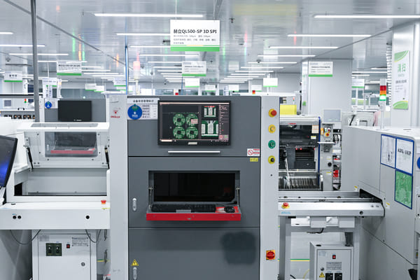
Solder Paste Inspection measures paste after stencil printing and before placement. A 3D SPI program checks height, area, volume, and offset, exposing paste shortage or excess, bridging, and print misalignment.
In AOI vs SPI vs X-Ray planning, SPI is the preventive gate. It cannot judge polarity, completed joints, or electrical behavior, but trends can guide stencil cleaning, alignment, squeegee settings, or aperture changes.
What Is AOI
Automated Optical Inspection uses cameras, lighting, and programmed criteria to check visible assembly features. It can find missing, reversed, shifted, or tombstoned parts, visible bridges, lifted leads, and abnormal solder fillets.
AOI vs SPI vs X-Ray comparisons often overstate AOI coverage. It needs line of sight, so it cannot inspect BGA joints or a QFN central pad, and it cannot prove circuit function.

What Is X-Ray Inspection
X-Ray inspection uses material thickness and density differences to image beneath opaque packages. It suits BGA, LGA, CSP, QFN, bottom-terminated devices, hidden bridges or opens, voiding, and selected barrel-fill concerns.
Within AOI vs SPI vs X-Ray, X-Ray supplies depth rather than broad coverage. Dense double-sided boards may create overlapping 2D features, so view and criteria must match the risk. X-Ray cannot verify part values or firmware.

AOI vs SPI vs X-Ray Differences and How They Work Together
AOI vs SPI vs X-Ray works best as three linked gates rather than three competing machines. The table shows what each gate proves and where its blind spot begins.
| Method | Process Gate | Checks | Finds Best | Does Not Prove |
|---|---|---|---|---|
| SPI | After printing, before placement | Paste height, area, volume, offset | Paste shortage/excess, bridging, print shift | Parts, reflow result, function |
| AOI | After placement and/or reflow | Visible parts and solder features | Missing/reversed parts, offset, tombstone, visible bridge | Hidden BGA/QFN joints, function |
| X-Ray | After reflow or during analysis | Hidden joint geometry and density | Hidden bridge/open, voiding, thermal-pad coverage | Part markings, firmware, full function |
If SPI shows paste drift, correct printing before placement. If AOI reports visible solder defects, review placement and reflow. Use X-Ray for a suspected hidden joint or to confirm a corrected hidden-joint process.
How to Choose AOI vs SPI vs X-Ray for a PCBA
Choose AOI vs SPI vs X-Ray from package visibility, defect risk, production stage, and the evidence needed for acceptance.
1. Standard SMT board: Use SPI for print control and AOI for visible defects. Add X-Ray for hidden features, first articles, or failure analysis.
2. BGA, QFN, LGA, or CSP: Plan X-Ray for concealed joints or thermal pads; AOI still checks orientation and placement.
3. Fine pitch or yield ramp: Correlate SPI and AOI data. Repeated related alarms indicate a process problem.
4. High reliability build: Set X-Ray scope based on product risk, lot history, and acceptance criteria: first articles, samples, critical packages, or every board.
5. Electrical or intermittent failure: Add flying probe, ICT, or functional testing. AOI vs SPI vs X-Ray does not verify powered behavior.
PCBgogo PCBA Quality Inspection Workflow
PCBgogo applies AOI vs SPI vs X-Ray as part of a layered PCBA quality workflow, with each result tied to a release decision rather than treated as a standalone report.
1. PCB design and manufacturing review: Review data, BOM, polarity, hidden pads, and acceptance requirements.
2. 3D SPI print verification: Use full-coverage SPI after printing to stop systematic print errors before placement.
3. Placement process setup: Confirm feeders, rotation, libraries, and first-article values.
4. AOI assembly inspection: Verify visible soldering, placement, missing parts, and polarity.
5. X-Ray internal verification: Inspect hidden BGA, QFN, and other high-density package joints to the agreed scope.
6. Engineering analysis and adjustment: Correlate findings, adjust printing, placement, or reflow, and confirm with new data.
7. Production readiness confirmation: Release after first-article results, criteria, defect handling, and required functional tests are confirmed.
PCBgogo - Reliable, High-Quality PCB Manufacturing
PCBgogo is a one-stop PCB and PCBA manufacturing factory, helping you save time and costs while ensuring consistent, reliable quality.
Get a Free Quote >
Conclusion
AOI vs SPI vs X-Ray is a sequence: SPI prevents paste defects, AOI controls visible quality, and X-Ray closes hidden-joint blind spots. Before production, define the process gate, inspected features, sampling scope, acceptance criteria, and records so each result supports a release decision.
AOI vs SPI vs X-Ray FAQ
Can AOI replace SPI
No. In AOI vs SPI vs X-Ray, AOI sees visible assembly results, while SPI measures paste before placement. Together they catch the source and confirm the result.
Does every PCBA need X-Ray inspection?
No. In AOI vs SPI vs X-Ray planning, X-Ray suits hidden joints, first articles, high-reliability builds, or failure analysis. Use targeted or sampled scope when process history and risk support it.
Can AOI vs SPI vs X-Ray guarantee a working PCBA?
No. AOI vs SPI vs X-Ray verifies physical process evidence, not complete performance. Electrical and functional tests must cover release behavior.