
 日本語
日本語

Most articles about 8-layer PCB stackups repeat the same diagram: signal, ground, signal, power, power, signal, ground, signal. It's not wrong — but it's also not the whole story. The layer count is the easy part. What actually determines whether an 8-layer board performs the way you expect is the order those layers go in, how reference planes are paired with the signals they protect, and whether the stackup was chosen to solve a specific problem or just copied from a template.
This article walks through how 8-layer stackups actually work, when 8 layers is the right call instead of 6 or 10, and what changes when the board has to survive somewhere harsher than a benchtop — like a vehicle or an industrial enclosure.
What Is an 8 Layer PCB Stackup, Really?
A stackup is the sequence of copper and dielectric layers that make up a multilayer board, laminated together under heat and pressure into a single rigid structure. An 8-layer stackup has eight copper layers separated by seven dielectric layers (a mix of core and prepreg material).
Four of those eight layers are typically used for signal routing, and the other four are dedicated ground and power planes. The planes aren't filler — they're what makes 8 layers behave differently from four separate 2-layer boards stacked on top of each other. A continuous ground plane directly beneath a signal layer gives every trace a low-impedance return path, which is the single biggest factor in controlling EMI and crosstalk on a dense board.
The Layer Sequence That Actually Works
There's no single "correct" 8-layer stackup — the right sequence depends on what the board needs to do. Two configurations cover most real projects:
General high-speed digital (routers, motherboards, controller boards)
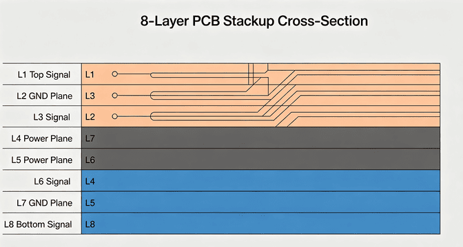
This arrangement keeps every signal layer adjacent to a plane, which is the rule that matters most: uninterrupted reference planes directly next to the layers carrying your fastest signals.
EMI-hardened variant (automotive, industrial, RF-adjacent designs)
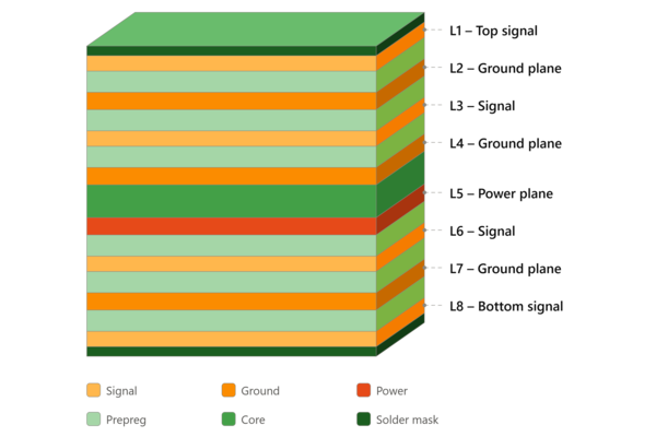
Adding a third ground plane sacrifices some routing flexibility but tightens shielding between sections — useful when the board sits near switching power electronics, motors, or RF sources, which is common in automotive and industrial environments.
How Stackup Order Affects Signal Integrity, EMI, and Power Delivery
Three effects come directly from layer order, not layer count:
Crosstalk control: signals routed on layers adjacent to a continuous ground plane have a tight, predictable return path. Move that same signal two layers away from its reference plane and crosstalk to neighboring traces climbs even though nothing else about the design changed.
Power plane pairing: placing the two power planes next to each other (as in the general-purpose sequence above) creates a thin, low-inductance capacitor between them, which helps with high-frequency decoupling before discrete capacitors even come into play.
Symmetry and warping: a stackup that isn't mechanically symmetric — copper weight and dielectric thickness mirrored around the centerline — is more likely to bow or twist during lamination and reflow. This is a fabrication problem, not just an electrical one, and it's one of the most common reasons a stackup that looked fine on paper causes yield issues at the factory.
Board Thickness and Material Selection
Total thickness for an 8-layer board typically lands between 1.57 mm (0.062 in) and 2.36 mm (0.093 in), though this varies with copper weight and dielectric choice. Copper is usually specified in ounces per square foot — 1 oz (about 35 μm) is standard, with 2 oz used where a plane needs to carry more current or spread more heat.
Standard FR-4 is sufficient for the majority of 8-layer designs. Two situations call for something more:
High-Tg FR4 or better, when the board will see repeated thermal cycling or reflow at elevated temperatures — common in automotive and industrial applications.
Low-loss or controlled-Dk laminates, when signals run fast enough (multi-gigabit serial links, RF sections) that ordinary FR-4's dielectric loss starts eating into your signal margin.
6, 8, or 10 Layers? A Practical Way to Decide
"It depends on complexity" isn't a useful answer. These four factors are what actually push a design from 6 to 8 layers, or from 8 to 10+:
| Situation | 6 Layers Usually Enough | 8 Layers Recommended | 10+ Layers Worth Considering |
|---|---|---|---|
| High-speed interfaces | 1–2 interfaces, moderate data rate | 3+ interfaces (DDR4, PCIe, USB 3.x together) | Multiple high-speed buses plus RF sections |
| Power rails | 1–2 rails, simple sequencing | 3–4 independent rails needing isolation | 5+ rails or mixed analog/digital domains |
| EMI environment | Benign, well-shielded enclosure | Automotive, industrial, or RF-adjacent | Safety-critical or regulatory-heavy (aerospace, medical) |
| Board size pressure | Room to spread components out | Dense BGAs, limited routing channels | Very dense, fine-pitch, mixed-technology boards |
If a design only trips one of these thresholds, it's often still workable on 6 layers with careful routing. Once two or more line up — say, three high-speed interfaces and a tight, EMI-sensitive enclosure — 8 layers stops being a nice-to-have and starts being the layer count that keeps the project out of a redesign.
Stackup Considerations for Automotive and Industrial-Grade Boards
Boards destined for a vehicle or an industrial control cabinet face conditions a consumer board never sees: continuous vibration, wide temperature swings, and long service-life expectations measured in years, not product cycles. That changes what matters in an 8-layer stackup:
Via reliability becomes a bigger deal than via density. Blind, buried, and via-in-pad structures reduce stress risers when they're executed with tight process control — poor drilling or plating in these vias is a common long-term failure point under thermal cycling.
Copper balance and symmetry matter more, since boards undergoing repeated thermal expansion and contraction are less forgiving of an asymmetric stackup than a board that lives in a climate-controlled enclosure.
Process discipline at the fab — consistent lamination, registration, and inspection — has an outsized effect on long-term reliability, which is why manufacturing quality systems (not just the stackup drawing) are part of the real decision for automotive-grade boards.
None of this changes the basic stackup logic from the sections above — it just raises the cost of getting it wrong, which is why automotive and industrial projects tend to lean on manufacturers with process discipline built around those requirements rather than general-purpose fabrication.
Common Stackup Mistakes That Cause Problems Later
Choosing a stackup off a template without checking it against the board's actual signal count, power rails, and enclosure environment
Leaving a signal layer without a continuous, adjacent reference plane
Building an asymmetric copper/dielectric arrangement that invites warping during lamination or reflow
Finalizing the stackup before checking it against the fabricator's real capabilities — drill aspect ratio, minimum trace/space, and via technology all constrain what's actually manufacturable
Skipping a DFM review before release, which is often where stackup mismatches with fabrication limits get caught
Where PCBgogo Fits Into an 8-Layer Project
PCBgogo fabricates multilayer boards up to 40 layers in-house, so an 8-layer stackup sits well within standard capability rather than at the edge of it. Boards are built on Shengyi laminates, following PCBgogo's move to Shengyi's high-performance substrates for better CAF resistance and thermal stability — relevant for the automotive and industrial stackups discussed above.
For the via structures that matter most in dense or EMI-sensitive 8-layer designs, PCBgogo supports laser-drilled microvias, blind and buried vias, and via-in-pad, backed by AOI and X-ray inspection on the production line. Every order goes through a DFM and engineer review before fabrication starts, which is the stage where a stackup choice gets checked against what's actually buildable — before it becomes an expensive lesson.
PCBgogo runs its own in-house facilities from fabrication through assembly, so an 8-layer stackup, an automotive-grade build, or a mixed prototype-to-production run all move through one factory rather than across multiple outsourced vendors. Standard 24-hour quick-turn options are available for prototype work, and native design files from Eagle, Altium, and PADS are accepted directly, which keeps the stackup information intact from CAD to fabrication. Certifications include IATF 16949, ISO 9001, RoHS, and UL. For project-specific quotes, PCBgogo's online instant quoting tool gives current, order-specific pricing rather than a general figure that goes stale.
Frequently Asked Questions
What is the standard layer sequence for an 8-layer PCB?
A common sequence is Signal – Ground – Signal – Power – Power – Signal – Ground – Signal, keeping every routing layer adjacent to a reference plane. The exact order should be adjusted for the board's specific signals and EMI environment.
How thick is a typical 8-layer PCB?
Most 8-layer boards fall between 1.57 mm and 2.36 mm, depending on copper weight and dielectric thickness. Thinner or thicker builds are possible with a custom stackup.
When should I move from 6 layers to 8 layers?
When a board needs to handle three or more high-speed interfaces, three or more independent power rails, or operates in an EMI-heavy environment like an automotive or industrial enclosure. One of these factors alone may still work on 6 layers; two or more together usually justifies 8.
Do 8-layer PCBs need blind or buried vias?
Not always. They become worthwhile when component density is high enough that through-hole vias would block routing channels, or when via stub length is hurting signal integrity on high-speed nets.
What material is best for an 8-layer high-speed board?
Standard FR-4 handles most designs. High-Tg FR4 is worth the upgrade for boards facing repeated thermal cycling, and low-loss laminates matter once signal speeds push into multi-gigabit territory.
Can I get a custom 8-layer stackup instead of a standard one?
Yes. Standard stackups are a starting point, not a requirement — most fabricators, including PCBgogo, will build a custom stackup once your DFM review confirms it fits their process capability.





